
Circuit Diagram
Index 330
L5991 shutdown function achieving circuit diagram
Published:2012/9/18 2:00:00 Author:Ecco | Keyword: shutdown function achieving
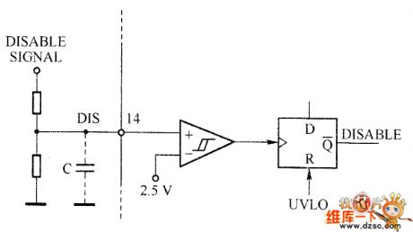
L5991's shutdown function is achieved by pin 14. When the voltage on the pin exceeds 2.5 V, the chip will be turned off, only VCC is pulled up to the UVLO threshold, the ffEF will has new start. The chip external force shutdown function can be achieved by the pin, and the circuit is shown in the figure. You can also use the pin to achieve overvoltage protection. In order to avoid the malfunction of this pin caused by noise spikes, in the actual using process, the circuit should bypass connect a thin film capacitor.
(View)
View full Circuit Diagram | Comments | Reading(780)
MAX1458 bridge excitation circuit diagram
Published:2012/9/18 2:21:00 Author:Ecco | Keyword: bridge excitation
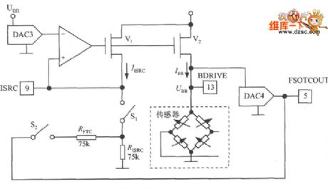
The bridge excitation circuit with digital pressure signal conditioner MAX1458 is shown as the figure. It uses DAC3 output to change the size of the sensor excitation current IBR and realize full-scale calibration. IISRC is the reference current set by RISRC and 9 feet voltage. V1 and V2 form a mirror current source, when the current gain is 14 times, the excitation current IBR = 14IISRC. The IBR programming range is 0.1 ~ 2mA. The on-off state of analog switches S1, S2 is governed by the configuration register. Obviously, when the full-scale output voltage changes, DAC3 will compensate bridge output voltage by BR changing, thereby correcting the errors of the full scale. DAC4 is used to correct the error of full scale temperature coefficient.
(View)
View full Circuit Diagram | Comments | Reading(743)
Basic JFET Pierce Crystal Oscillator
Published:2012/9/17 21:42:00 Author:Ecco | Keyword: Basic , JFET, Pierce , Crystal Oscillator

This circuit is a series of JFET Pierce Crystal Oscillator. JFET Pierce crystal oscillator allows a wide range of crystal frequencies to be used without modification of the circuit. Since the JFET gate did not contain crystals, Q both maintained that insure a good frequency stability. (View)
View full Circuit Diagram | Comments | Reading(3314)
Simple 555 Timer Monostable Circuit
Published:2012/9/17 21:41:00 Author:Ecco | Keyword: 555 , Timer, Monostable
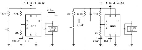
The two circuits below illustrate using the 555 timer to close a relay for a predetermined amount of time by pressing a momentary N/O push button. The circuit on the left can be used for long time periods where the push button can be pressed and released before the end of the timing period. For shorter periods, a capacitor can be used to isolate the switch so that only the initial switch closure is seen by the timer input and the switch can remain closed for an unlimited period without effecting the output. (View)
View full Circuit Diagram | Comments | Reading(2286)
Dual Precision Monostable Logic circuit (CD4538BC)
Published:2012/9/17 21:41:00 Author:Ecco | Keyword: Dual, Precision Monostable , Logic circuit
The logic diagram of the CD4538BC Dual Precision Monostable is shown in the following schematic diagram. This IC such a dual, precision monostable multivibrator with independent trigger and controls, according to the datasheet. This CD4538BC IC features wide supply voltage range, wide pulse-width range, low standby current, high noise immunity and more. (View)
View full Circuit Diagram | Comments | Reading(632)
Simple Wien-Bridge Oscillator
Published:2012/9/17 21:40:00 Author:Ecco | Keyword: Simple, Wien-Bridge Oscillator

Incandescent lamp has been used to reduce harmonic distortion in sine oscillator circuit. The nonlinear resistance characteristic of the lamp filament help the circuit to shape the signal to approximate the ideal sine wave. Here is the classic Wien-bridge oscillator circuit using the incandescent lamp.
Source: freecircuitdiagram (View)
View full Circuit Diagram | Comments | Reading(0)
Voltage Controlled Oscillator 1.2GHz
Published:2012/9/17 21:38:00 Author:Ecco | Keyword: Voltage Controlled Oscillator, 1.2GHz
Since high frequency voltage-controlled oscillators, or VCOs, are not easy to construct, Maxim (www.maxim-ic.com) has produced an integrated 1.2GHz oscillator, the MAX2754. The center frequency is set using the TUNE input, and a linear modulation input allows the frequency to be modulated. The IC is available in an 8-pin μMAX package, operates from a supply of between 2.7 V and 5.5 V, and draws a current of less than 2 mA. Both TUNE and MOD operate over control voltage range of +0.4 V to +2.4 V. TUNE allows the VCO frequency to be adjusted from 1050 MHz to 1270 MHz. (View)
View full Circuit Diagram | Comments | Reading(868)
Astable/Monostable oscillator using 555 IC
Published:2012/9/17 21:37:00 Author:Ecco | Keyword: Astable/Monostable oscillator , 555 IC
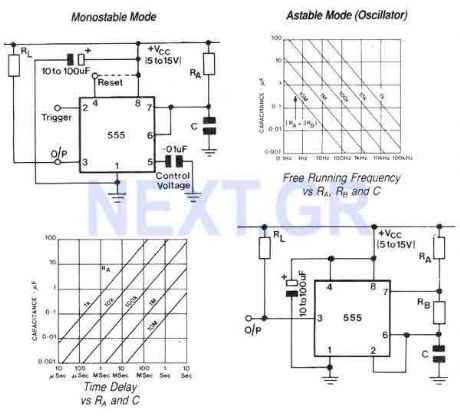
The 555 is a highly stable device for generating accurate time delays or oscillation. Aditional terminals are provided for triggering or resetting if desired. In the time delay (monostable) modeof operation the time is precisely controlled by one extrernal resistor and one capacitor. For stable operation as an oscillator, the free running frequency and the duty cycle are both accurately controlled with two external resistors and one capacitor. (View)
View full Circuit Diagram | Comments | Reading(1095)
Square Wave Generator with CMOS 74C14
Published:2012/9/17 21:33:00 Author:Ecco | Keyword: Square Wave Generator, CMOS
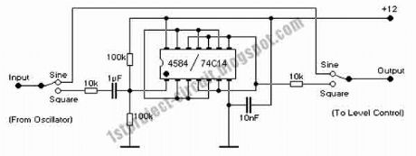
This circuit is based on CMOS IC 74C14. The output of this circuit is from 0V to +12V, and is fed to the 10k level pot by a 10k resistor. This reduces the level to 6V P-P, which is equal to 3V RMS. The input circuit is designed to ensure that the Schmitt input is supplied from a 1/2 supply voltage (6V), so the applied AC will swing evenly about this point and produce a symmetrical square wave.
(View)
View full Circuit Diagram | Comments | Reading(1565)
Adjustable Sine Square Wave Oscillator
Published:2012/9/17 21:31:00 Author:Ecco | Keyword: Adjustable, Sine Square Wave, Oscillator
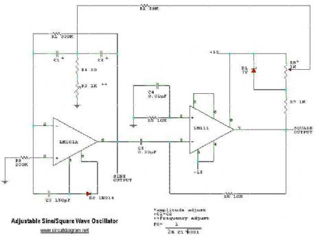
This is a adjustable sine square wave oscillator circuit. (View)
View full Circuit Diagram | Comments | Reading(1471)
RF oscillator circuit (2N3904)
Published:2012/9/17 21:31:00 Author:Ecco | Keyword: RF oscillator
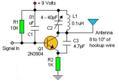
This basic RF oscillator circuit is easy to build and the components are not critical. Most of them can be found in your junk parts box. The L1 antenna col can be made by close winding 8 to 10 turns of 22 gauge insulted hookup wire around 1/4 inch form such as a pencil. (View)
View full Circuit Diagram | Comments | Reading(5122)
100 MHz RF Oscillator Circuit
Published:2012/9/17 21:30:00 Author:Ecco | Keyword: 100 MHz , RF Oscillator
The following schematic diagram shows the design of a 100 MHz Radio Frequency RF Oscillator Circuit. The electrets microphone picks up and amplifies sound then fed it into the audio amplifier stage built around the first transistor. The output from the collector is fed into the base of the second transistor where it modulates the resonant frequency of the tank circuit (the 5 turn coil and the trim cap) by varying the junction capacitance of the transistor. (View)
View full Circuit Diagram | Comments | Reading(1371)
Basic Hartley Oscillator
Published:2012/9/17 21:30:00 Author:Ecco | Keyword: Basic , Hartley Oscillator
The Hartley Oscillator is characterised by an LC circuit in its collector. The base of the transistor is held steady and a small amount of signal is taken from a tapping on the inductor and fed to the emitter to keep the transistor in oscillation. (View)
View full Circuit Diagram | Comments | Reading(1168)
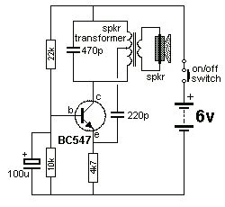
Speaker protection circuit
Published:2012/9/17 1:19:00 Author:Ecco | Keyword: Speaker, protection circuit

The speaker protection circuit is shown in the figure. It has the left and right channels to work independently. In the Figure ( left channel ), R2 , C4, VT2 and VT3 form a starting up delay circuit to prevent the starting up high-current impact on speaker.
Components Selection: LED can choose Φ3mm high-brightness color LED. Since LED current may be high or low, the parameters of R5, R9 can be slightly adjusted. At the same time, the LED and the current limit resistors R5, R9 are connected to two ends of relays RE1 and RE2 in parallel to inhibit the anti-peak voltage and prevent the breakdown from VT2, VT3, VT5 and VT6. C4, C9 should use low-leakage tantalum capacitors. Other components parameters are shown in the figure.
(View)
View full Circuit Diagram | Comments | Reading(4227)
The annular scintillator schematic
Published:2012/9/17 1:08:00 Author:Ecco | Keyword: annular scintillator
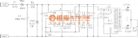
The circuit is mainly composed of NE555, CD4017 and peripheral circuits. The NE555 forms multivibrator, and its pin 3 outputs square wave to control CD4017 output shift end and individually light LED so that the LED ring flashes. As shown in the figure, the line flicker frequency is about 1.5Hz, operating current is less than 50mA.
Components Selection: IC1 chooses the 555 tine-base circuit, IC2 selects CD4017 integrated circuit. R1 uses (1/2) W metal film resistor, the remaining resistors selects (1/4) W resistors, LED0 ~ LED9 can choose Φ5mm ultra bright or special highlight red light-emitting tube. Other components are shown as the figure.
(View)
View full Circuit Diagram | Comments | Reading(1302)
The level test circuit with CMOS NAND gate 4011 connected into inverter
Published:2012/9/16 22:53:00 Author:Ecco | Keyword: level test , CMOS NAND gate , inverter

In this circuit, it can also use NOT gate to replace 4011. High level displays H, low level displays L. R2 ~ R4 play a limiting role, so the digital tube and its anode are connected to the positive power supply Vcc directly. The normally on segments e , f are grounded by R4 to reduce the drive current.
(View)
View full Circuit Diagram | Comments | Reading(1997)
Frequency shift keying modulation and demodulation circuit with XR-2207
Published:2012/9/17 1:28:00 Author:Ecco | Keyword: Frequency shift, keying modulation , demodulation

XR-2207 is a a voltage - controlled oscillation (VCO) function generator integrated circuit, and it is used as modulation and demodulation circuit to generate rectangular wave and triangular wave (but it can not generate sine wave ).
(View)
View full Circuit Diagram | Comments | Reading(2229)
The test signal generator using modulator circuit
Published:2012/9/17 1:32:00 Author:Ecco | Keyword: test signal generator , modulator
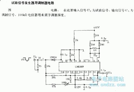
In the circuit shown as figure, it is input signal UE as test signal, the output signal UA is modulation signal, 100 KΩ potentiometer is used to adjust modulation depth.
(View)
View full Circuit Diagram | Comments | Reading(835)
Notching filter circuit with variable Q
Published:2012/9/13 22:49:00 Author:Ecco | Keyword: Notching filter , variable Q

A notch filter circuit with a variable quality factorThe notch filter circuit uses two LM110 or SN72310 operational amplifiers as voltage follower, and the circuit is shown in figure.
(View)
View full Circuit Diagram | Comments | Reading(1097)
Four-stage telecom filter circuit with 1KHZ frequency
Published:2012/9/13 22:43:00 Author:Ecco | Keyword: Four-stage , telecom, filter , 1KHZ frequency

Third-order asymmetric filter circuit has two ways of output UA1 and UA2, the former is high-pass filter output, and the later is low-pass filter output.
(View)
View full Circuit Diagram | Comments | Reading(1250)
| Pages:330/2234 At 20321322323324325326327328329330331332333334335336337338339340Under 20 |
Circuit Categories
power supply circuit
Amplifier Circuit
Basic Circuit
LED and Light Circuit
Sensor Circuit
Signal Processing
Electrical Equipment Circuit
Control Circuit
Remote Control Circuit
A/D-D/A Converter Circuit
Audio Circuit
Measuring and Test Circuit
Communication Circuit
Computer-Related Circuit
555 Circuit
Automotive Circuit
Repairing Circuit