
Circuit Diagram
Index 328
BC546, BC547, BC548, BC549, BC550 Datasheet
Published:2012/9/18 21:36:00 Author:Ecco | Keyword: Datasheet
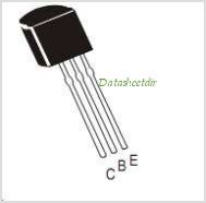
BC546, BC547, BC548, BC549, BC550 are NPN switching and amplifier transistors with low noise and working at high voltage.
Pinout configuration (View)
View full Circuit Diagram | Comments | Reading(3210)
TL496 datasheet
Published:2012/9/18 21:36:00 Author:Ecco | Keyword: datasheet
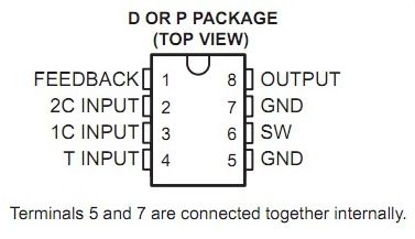
The TL496C power-supply control circuit is designed to provide a 9-V regulated supply from a variety of input sources. Operable from a 1- or 2-cell battery input, the TL496C performs as a switching regulator with the addition of a single inductor and filter capacitor. When ac coupled with a step-down transformer, the TL496C operates as a series regulator to maintain the regulated output voltage and, with the addition of a single catch diode, time shares to recharge the input batteries.The design of the TL496C allows minimal supply current drain during standby operation (125 μA typical). With most battery sources, this allows a constant bias to be maintained on the power supply. This makes power instantly available to the system, thus eliminating power-up sequencing problems.
(View)
View full Circuit Diagram | Comments | Reading(755)
Simple pulse position modulation circuit
Published:2012/9/18 21:36:00 Author:Ecco | Keyword: Simple pulse , position modulation
In pulse position modulation, the amplitude and width of the pulses are kept constant, while the position of each pulse with reference to position of reference pulse, is changed according to the instantaneous sampled value of the modulating signal. Below shown circuit diagram is the simplest pulse position modulation circuit using IC-555.
With this type of circuit, the position of each pulse changes. Both width and period of the pulses vary with the modulating signal. Due to modulating signal at pin 5 ( Control voltage pin ), the UTP level changes to (2Vcc/3)+Vmod.
When Vmod increases, the UTP level increases and hence pulse width also increases. If Vmod decreases, UTP level decreases and pulse width also decreases. Thus the pulse width varies.
The pulse width is given by,
W = – (R1+R2) Cin [ (Vcc-UTP)/(Vcc-0.5UTP) ].
The period is given by,
T = W+0.693R2C
The space between the pulses which is constant is given by 0.693 R2C.This circuit has many application a quick example is, it is used in communication application for transferring voice or data.
One Response to “Simple pulse position modulation circuit”
(View)
View full Circuit Diagram | Comments | Reading(560)
High temperature indicator circuit
Published:2012/9/18 21:35:00 Author:Ecco | Keyword: High temperature, indicator
In some areas there is a need of temperature detectors which help them to detect temperature and indicate them?whether the temperature is low or not.
Below shown circuit is the simple high temperature indicator circuit. It will not show the current temperature but if it exceeds some threshold temperature it will detect and indicate. You can use this circuit anywhere you needed.
The components needed for the circuit are:
3 Resistors
1 Temperature dependent resistor
5v battery
Two 1n4007 diodes
One Op-Amp
One LED
And the circuit working is actually very simple, the Op-amp is connected as Non-inverting comparator. And a bridge circuit is made with the resistors and a Temperature Dependent Resistor. From above circuit R1, R2 and R3 are normal resistors but RT is Temperature Dependent Resistor.
The bridge resistance and RT are selected in such a way that as long as temperature is less than threshold value, the bridge is unbalanced by making Voltage at B more than voltage at A . Hence Vo = -Vsat and LED is reverse biased and remains OFF. When temperature becomes more than threshold then Voltage at B becomes less that Voltage at A hence it drives Vo = +Vsat. Due to this, LED glows and gives high temperature indication.
If you have any doubts about the above circuit, don’t hesitate to comment.
One Response to “High temperature indicator circuit”
(View)
View full Circuit Diagram | Comments | Reading(1146)
Single 1.2V NiMH Cell LEDs Flashlight
Published:2012/9/18 21:35:00 Author:Ecco | Keyword: Single, 1.2V , NiMH Cell, LEDs Flashlight
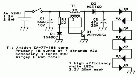
The single cell led flashlight circuit is a self-oscillating boost converter. A typical white LED has its best power-efficiency combination at about 20mA, and needs about 3.3V. This makes for a power of about 66mW per LED. In this circuit are 7 series LEDs so we need a driver circuit that will provide about 23V at 20mA, when fed from a 1.2V NiMH rechargeable cell or from a 1.5V alkaline cell.
When switching it on, R1 and D1 bias the transistor into the linear range, through the feedback winding on T1. That causes a current through the 18 turn winding, and thanks to the positive feedback the transistor is driven into saturation. At this moment there will be a base current defined like this: The 1.2V of the cell, plus the 0.2V induced in the feedback winding, minus the 0.7V base-emitter drop of the transistor, make a total of 0.7V, which applied to the 22 ohm resistor gives about 32mA base current. D1 is not conducting a significant current at this time, because the transistor clamps the base voltage to 0.7V and the 3 turn winding subtracts 0.2V from this, so that we end up with only 0.5V across the diode.
This base current keeps the transistor in saturation until its collector current reaches approximately 1A, while the transformer loads up. At this point the transistor will start getting out of saturation, which makes the feedback voltage drop. This very quickly puts the transistor into blockage. The collector voltage will soar as T1 forces current to keep flowing, until D2 starts conducting and discharges the transformer into C2, by means of a quite narrow pulse. During operation this pulse is about 24V high, so that the feedback winding develops -4V, which results in applying about -3.3V to Q1′s base, enough to switch it off very fast, but not enough to make the base reverse-conduct.
As soon as the transformer has fully discharged into C2, the voltage on it breaks down, and the transistor enters conduction to start a new cycle. The oscillating frequency is 30kHz, and the transformer operates at a peak flux density of 0.1 tesla, far away from saturation, and low enough to have very low loss. C2 has to eat the load pulses that start at about 1A, and has to keep the voltage constant enough to feed the LEDs an almost smooth DC. The value given works well. If anyone wants to build this circuit to run 24 hours a day for 30 years, it would be good to pick a capacitor rated for low ESR and a relatively high ripple current, but for flashlight use a plain standard 47μF, 35V electrolytic capacitor works great.
C1 is not strictly necessary. With a good NiMH cell, the circuit works the same without it, so you can save a few cents here. But with the capacitor in place, the circuit keeps working better when the cell is almost fully discharged and its internal resistance gets higher, so it’s better to include it.
Source: http://ludens.cl/Electron/ledlamp/ledlamp.html
2 Responses to “Single 1.2V NiMH Cell LEDs Flashlight”
(View)
View full Circuit Diagram | Comments | Reading(1804)
Automatic street light circuit
Published:2012/9/18 21:34:00 Author:Ecco | Keyword: Automatic street light

There have been lot of problems in street lights. Major problem in some places is every evening a person has to come and switch ON the street light and it should be again switched off in morning. Yes, this may not be the situation in everywhere but exists in many places.So this problem can be overcome by using a simple circuit. Below shown circuit will be automatically switched ON and OFF during night and morning times respectively.
Automatic light schematic
In above circuit R1 can be used to adjust the sensitivity. And the working of the circuit is very simple. The LDR will have very low resistance during day time so the transistor Q1 will be in OFF condition. And during night time the resistance will be very high so automatically the transistor Q1 will be ON.
The Q1 is PNP transistor and the emitter of Q1 is given to base of Q2. So the Q2 transistor will be ON only if the transistor Q1 is ON. The TRIAC is used in the circuit to make is circuit complete. As the TRIAC will allow voltage to pass from either directions only when there is a certain threshold voltage in gate terminal. And the gate of TRIAC is controlled by transistor Q2.
So totally the lamp will be ON during night time and will be again switched off during day light. To change the sensitivity of the circuit to light adjust R2.
If you have any doubts, do not hesitate to comment below. We will come to you with an appropriate solution.
19 responses to “Automatic street light circuit”
(View)
View full Circuit Diagram | Comments | Reading(1288)
Automatic Light Switch with PhotoTransistor
Published:2012/9/18 21:34:00 Author:Ecco | Keyword: Automatic Light Switch, PhotoTransistor
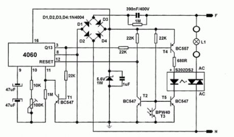
This is an automatic light switch circuit that turns ON a light bulb in absence of light. The IC 4060 works as an oscillator and generates a signal that is applied to the base of T4 transistor. Phototransistor T3 BPW40 is in conduction when light is present and it keeps the T5 transistor’s base at ground potential.When light goes out and it doesn’t reaches the phototransistor, it gets in insulation. T3 reaches positive potential through 22kohm. T4 and T5 both gets in conductance. The oscillator signal reaches the optic coupler and then turns on the lamp.
2 Responses to “Automatic Light Switch with PhotoTransistor”
(View)
View full Circuit Diagram | Comments | Reading(2023)
USB Power Booster
Published:2012/9/18 21:33:00 Author:Ecco | Keyword: USB, Power Booster


As you probably know, the USB 2.0 ports can deliver up to 500 mA, that means about 2.5W. But sometimes you might need more power to connect an external HDD or other peripherals and the USB ports just cannot deliver enough current. In this case you can buy USB hubs that have an external power adapter required to boost the power or you can build a simple or complex circuit that can do the same thing.
There are many usb power booster projects available on the internet, some of them are very complicated, others are simple as using a few components. One simple design involves the use of the 7805 voltage regulator that can deliver 5V and 1A.
Circuit No 1I have found this design on Electronics For You website and it uses the 7805 regulator, a MOC3021 optoisolator as main components. (source)
Circuit No 2This is another design that uses LM2575-5 step-down switching voltage regulator. Its principle is that internal power transistor switch on and off according to a feedback signal. This chopped or switched voltage is converted to DC with a small amount of ripple by D1, L1 and C2.
Circuit No 3This usb power booster circuit is the simplest one and it uses the 7805 voltage regulator that can deliver up to 1A.
Circuit No 4It uses the same 7805 but with 2 external transistor it can deliver up to 3 amps, that is 15W of power (source).
Of course you will need an external adapter to power up this circuits, something like a 12V DC adapter. What do you think?
Source: electroschematics.com
(View)
View full Circuit Diagram | Comments | Reading(1684)
First-order butterworth active low-pass filter
Published:2012/9/18 21:33:00 Author:Ecco | Keyword: First-order butterworth, active, low-pass filter
Butterworth filter is a type of filter whose frequency response is flat over the passband region. Low-pass filter (LPF) provides a constant output from DC up to a cutoff frequency f(H) and rejects all signals above that frequency. Circuit diagram shown below is a first-order low-pass Butterworth filter that uses RC network for filtering. Loading of the RC network is avoided by using the Op-Amp which is configured for non-inverting mode. Resistors R1 and Rf determine the gain of the filter.
Op-Amp ( 5 terminal )
3 Resistors
1 Capacitor
Voltage sources
Af = 1+Rf/R1
f (H) = 1/(2πRC)
In the above circuit the component XSC1 is the Oscilloscope which is used to verify the circuit so don’t get confused with it. In the above circuit the cutoff frequency is decided the resistor R and capacitor C. You can choose any desired value to fix the cutoff frequency. In the above circuit i choose the cutoff frequency to be approximately 5KHz so i used the resistor R of value 10KΩ and capacitor of value 3nF. You can change it if you want to by using the above cutoff frequency formula.
The first order low-pass filter has a practical slope of -20 dB/decade. The low-pass filter has a constant gain Af from 0 to high cutoff frequency f (H). At f(H) the gain is 0.707Af and after f (H) it decreases at a constant rate of 20 dB/decade. The frequency f = f (H) is called the high cutoff frequency because the gain of the filter at this frequency is down by 3 dB ( =20log(10) 0.707 ) from 0 Hz.
The AC analysis of the above circuit is given below. But it is not exactly for the above circuit. The cutoff frequency is now made 20kHz. For getting cutoff frequency 20kHz you need resistor of value 1KΩ and capacitor of value 7.96nF.
If you have any doubt in the circuit please let us know by comments.
2 Responses to “First-order butterworth active low-pass filter”
(View)
View full Circuit Diagram | Comments | Reading(802)
Cell Phone charger using 1.5V battery
Published:2012/9/18 21:32:00 Author:Ecco | Keyword: Cell Phone charger, 1.5V battery

This article was received from Subham Chatterjee. Thank you!
For the cell phone to charge, charger output must be above 4V and can deliver a maximum current of 500mA. This charger circuit will step up the voltage from 1.5V to 5V DC to reach the cell phone charging requirement. The circuit uses only an AA or AAA 1.5v battery (1V to 2.4V). The charger is composed of simple oscillator, a rectifier, and voltage regulator.The feedback winding F is composed 5 turns of #30 AWG magnetic wire and main winding P is composed of 6 turns of #24 AWG wire. The 5.1V zener diode and 2200uF capacitor regulates the output voltage to ensure proper charging.
The windings are not critical, you can experiment using different number of turns. If ever the charger doesn’t have any output, try to reverse the winding connection.
Cellphone charger circuit schematic
My opinion is that this can charge the cellphone battery only for short period of time because the 1.5 volt battery power capacity is much lower than the phone’s battery.
17 Responses to “Cell Phone charger using 1.5V battery”
(View)
View full Circuit Diagram | Comments | Reading(2177)
LED Driver with 555 Timer
Published:2012/9/18 21:31:00 Author:Ecco | Keyword: LED Driver , 555 Timer

This simple LED driver circuit allows us to drive up to seven LEDs by using a single NiMH (Nickel Metal Hydride) AA cell. The circuit produces voltage pulses at a much higher level than the input supply voltage by pulsing the 220 uH inductor. The inductor must be a high Q (Q>90) power inductor. When the input is 1.25 V and the LEDs are connected, the voltage pulse level will be 23V.The LED driver uses a CMOS 555 timer since it operated with low voltages and can work for about 190 hours when using a single NiMH battery cell rated at 2000 mAh. The 555 timer drives the transistor at 222 kHz rate.
The seven LED groups can be connected paralelly if their forward voltages match. If not, the LED group with the lowest forward voltage value will dim out the other group(s). This parallel connection will not affect the total current drawn from the battery but it will reduce the brightness of the LEDs.
LED Driver Circuit Schematic
When a single 1.25V cell is used, the seven LED group will draw about 8mA from the battery. When the input value increases to 2.5V, the total drawn current will be 20mA.
5 Responses to “LED Driver with 555 Timer”
(View)
View full Circuit Diagram | Comments | Reading(3491)
Precision full wave rectifier circuit
Published:2012/9/18 21:31:00 Author:Ecco | Keyword: full wave rectifier
The use of Operational amplifiers can improve the?performance?of a wide?variety?of signal processing circuits. In rectifier circuits, the voltage drop that occurs with an ordinary semiconductor rectifier can be eliminated to give precision rectification.The below shown circuit is the precision full wave rectifier. It consists of following sections:
The input voltage Vin is applied to one terminal of the summing amplifier along with resistor R3 and to the input of the precision rectifier. The output of precision rectifier is applied to another terminal of summing amplifier. The precision half-wave rectifier circuit uses an inverting amplifier configuration.
When the input signal Vin is positive, Op-Amp output terminal is negative, Diode D1 is reverse biased and D2 Diode is forward biased, the circuit is
Vb = -(R2/R1) * Vin
In the circuit, R1 and R2 have been chosen such that R2 = 2R1.So the voltage at Vb = -2Vin.
Thus during the positive half cycle of the rectified voltage Vb is applied to terminal B of the inverting summing amplifier is -2Vin.
The voltage at terminal A is Va = +Vin. The output from the summing circuit with R3=R4=R5 is Vo = – (Va+Vb). Hence Vo = -(Vin – 2Vin) = +Vin. So during the negative half cycle of the input, the Op-Amp output terminal goes positive, causing D2 to be reverse biased. Without D1 in the circuit, the Op-Amp output would be saturated in the positive direction. However, the positive voltage at the Op-Amp output forward biases the D1. This tends to pull the Op-Amp inverting terminal in a positive direction. But, such a move would cause the Op-Amp output to go negative. So, the output settles at the voltage close to ground level. So to be clear, the negative half-cycle is clipped off. That is Vb=0 and Va = -Vin. Totally the Vo will be ?Vo = -(-Vin+0) = +Vin.
It is seen that the output is a full wave rectified version of the input voltage. A Precision full-wave rectifier is also known as absolute value circuit. This means the circuit output is the absolute value of the input voltage regardless of polarity.
If you any doubt about the circuit please drop it in comments we will respond you.;2 Responses to “Precision full wave rectifier circuit”
(View)
View full Circuit Diagram | Comments | Reading(0)
LA4440 datasheet
Published:2012/9/18 21:30:00 Author:Ecco | Keyword: datasheet
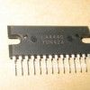
LA4440 is a 2 channel power amplifier that can deliver up to 6W per channel of 19W in bridge connection. It requires minimum number of external parts, it has small pop noise at the time of power supply ON/OFF. It has good ripple rejection of 46dB, small residual noise, built in over voltage and surge voltage protection etc. ideal feature of the IC is its pin-to-pin protection.LA4440 Features
Good ripple rejection : 46dB (typ.)
Good channel separation.
Small residual noise (Rg=0).
Low distortion over a wide range from low frequencies to high frequencies.
Easy to design radiator fin.
Built-in audio muting function.
Built-in protectors.
Thermal protector
Overvoltage, surge voltage protector
Pin-to-pin short protector (View)
View full Circuit Diagram | Comments | Reading(813)
3V to 9V DC Converters
Published:2012/9/18 21:30:00 Author:Ecco | Keyword: 3V to 9V, DC Converter

Here are some 3V to 9V DC converter circuits that were requested by some of our visitors. It may be helpful to have one of this converters when no 9V battery is available or if you consider that they are too expensive. The first circuit is very simple, it uses the TL496 power supply controller, a coil and a electrolytic capacitor.TL496 3 to 9 volt converter circuit
The maximum output voltage is actually 8.6V and current is around 80mA.The input current (the current drawn from the batteries) is 405mA at the maximum output current. Without load the current consumption is 125µA and the batteries life is around 166 days.
Here is another 1.5… 4.5V to 9V converter
3 volt to 9 volt with LMC555This dc converter is built with the CMOS version of 555 timer. You can get 12V too if you change the zener diode to a 12V version.
Probably there are more 3 to 9 volt dc converters but for the moment those are the only ones presented in this article.
2 Responses to “3V to 9V DC Converters”
(View)
View full Circuit Diagram | Comments | Reading(3472)
How to move a trip point of Op-Amp comparator Circuit
Published:2012/9/18 21:29:00 Author:Ecco | Keyword: How to move , trip point , Op-Amp comparator

You all will be?familiar of basic comparator using a Op-Amp circuit. So today we will show you how to move a trip point of a Op-Amp comparator circuit. Maybe many of people already know this, but still this is the post for?beginners. So if you already know quit reading now only.
As shown in the above circuit, by application of a reference voltage to the inverting input rather than grounding it the trip can be moved. The reference voltage is given to the inverting input of a basic comparator using a potential divider consisting of resistors R1 and R2. The reference voltage Vref is derived using +Vcc and potential divider R1 and R2. Mathematically Vref is expressed as,
Vref = [+Vcc/(R1+R2)] R2
Now as long as the input voltage is less than Vref, the output is low i.e. -Vsat. When Vin becomes slightly greater than Vref, the Op-Amp output becomes high i.e. +Vsat. Thus the trip point is moved from Vin = 0 to Vin = Vref due to reference voltage applied to the inverting input terminal.
A bypass capacitor is used on the inverting input to reduce the amount of power supply ripple and noise appearing at the inverting input of Op-Amp. For effective bypassing of ripple and noise, the critical frequency of bypass circuit must be much lower than the ripple frequency of power supply.
The transfer characteristics of such a comparator is shown in above diagram which indicates positive trip point. Such a comparator is also called a limit detector as it detects the particular positive level of the input beyond which input goes high. The resistance R1 and R2 can be used to set the trip point anywhere between 0 and +Vcc.
The cut-off frequency of bypass circuit is,
fc = 1/[ 2π(R1||R2) Cby.
This must be much lower than the ripple frequency of the supply.10 Responses to “How to move a trip point of Op-Amp comparator Circuit?”
(View)
View full Circuit Diagram | Comments | Reading(734)
Basic low power AM transmitter
Published:2012/9/18 21:26:00 Author:Ecco | Keyword: Basic, low power , AM transmitter
This transmitter?is basic but allows transmission of audio to an AM radio. It consists of an RF?oscillator operating in the AM broadcast band, together with a modulator stage,?which mixes the incoming audio and the RF. A signal appears on the output, which?has an AM component that can be picked up on a nearby AM radio receiver.
The transmitter consists of?oscillator stage Q1 and modulator/buffer stage Q2. Q1 is biased via R1, R2, and R3.?L1, C3, and C4 form the tank circuit with feedback network C3-C4 providing feedback?to the emitter of Q1. RF voltage at the junction of C3 and L1 drives buffer/modulator stage Q2. Q2 is biased by base current produced by RF rectification in the?base emitter junction of Q2. C6 is an RF and AF bypass capacitor. C9, C10, and L2?form the tank circuit for the collector of Q2. RF is taken from the junction of C9 and?C10 and fed to a?short-wire?antenna. Audio is fed to modulator Q2 via C8 and isolation?resistor R5 and mixes with the RF signal in the collector circuit of Q2, producing?a signal that has sum and difference frequencies if the RF carrier and AF input ?along with the carrier signal.
An AM signal appears at?the collector of Q2. Audio with an RMS voltage equal to about 0.7 times the collector?voltage of Q2 is needed for full modulation of the output.?Because of the high level of audio needed, the modulation obtained from this circuit?is somewhat limited with conventional audio sources because several volts of?audio into a few hundred ohms is needed. The circuit demonstrates the principle of?an AM transmitter, however, and with a suitable audio drive level, produces a well modulated?AM signal.5 Responses to “Basic low power AM transmitter”
(View)
View full Circuit Diagram | Comments | Reading(1872)
Temperature relay circuit
Published:2012/9/18 21:25:00 Author:Ecco | Keyword: Temperature relay

This simple temperature relay circuit can be used to signal a fire or setpoint for temperature monitoring function. You need to adjust P1 so that T1′s base voltage is 0.5V smaller than the emitter voltage at a temperature a little bit lower than the desired triggering (switching) temperature.If the temperature increases then T1 and T2 start conducting and the relay is closed (ON). If you want to use it as a cold relay or to signal an inferior temperature limit, then Th1 and P1 change places. After the relay is triggering you need to open switch S1 in order to stop the circuit. The nominal value of P1 must be choosed according to the used NTC thermistor and the switching temperature to be adjusted.
Temperature relay schematic
T1 can be BC557 and T2 BC547.
One Response to “Temperature relay circuit”
Source: electroschematics.com
(View)
View full Circuit Diagram | Comments | Reading(1592)
12V SCR Battery Charger
Published:2012/9/18 21:25:00 Author:Ecco | Keyword: 12V , SCR Battery Charger

This battery charger circuit differs from the norm in a number of ways, all of which make it difficult to understand. For this reason, I do not recommend it for the beginner.Repairing /revamping a dead chargerWhat I started with was an inoperative 12amp battery charger. In hope of repairing it, I traced out the circuit, but did not like what I found—poor circuit design. So what I had to start with was an enclosure, ammeter, thermal overload interrupter, and center-tapped transformer all designed for battery charger application.
Since the maximum current delivered by the unit is a function of the transformer internal impedance, I recommend that the readers use the same type of transformer. If you are a good pack-rat (like me), you may already have a dead charger—or you can be on the lookout for one.
12V Battery Charger Schematic
SCR (Thyristor) RectifiersFirst of all, the two SCRs (silicon controlled rectifiers or thyristors) are connected with their anodes (stud or tab) grounded—this makes for excellent thermal transfer because no insulating hardware is required (if it is permissible to connect the negative terminal of the charger directly to the steel enclosure). If you do not wish to ground this point, use insulating hardware to electrically isolate the SCRs. This makes the transformer center-tap the positive terminal. The reason for this circuit placement is the ease of driving the SCR gates via the positive battery voltage—it is very unconventional as I have never seen this trick done before.
SCRs are the ideal power device choice for a battery charger because they can both regulate battery charging voltage and prevent fault current when the battery is inadvertently connected reverse. I have actually connected mine reverse and thought that the charger was inoperative until I realized what I had done.
Power Device SelectionI used two 2N690 stud-mount SCRs that I had available. Any in the series will work (2N683 through 2N690)—only the voltage rating differs and anything greater than 100V is good for the application. Other more inexpensive TO-220 candidates are: STMicroelectronics TYN616, Teccor/Littlefuse S6015L (isolated package), NXP 151-500C, or ON Seimconductor 2N6403G. Avoid sensitive gate devices.
Circuit CommonNormally circuits use a negative common—that is just the way the world seems to work, but in this case, it was more convenient to make the positive rail the common point and all visualization must be made with this in mind. The only exception is D7 that was installed to prevent damage should the battery get connected reverse. For visualization, simply short out D7. The conventional ground symbol is used for the negative rail. This tends to tie your brain in knots…
Voltage ReferenceA good battery charger tapers off when the battery voltage is above about 14V. For this to function, D6 is a 5.1V shunt zener regulator that puts out -5.1V relative to the positive rail. It is biased via R8.
Ramp GeneratorC1 and R4 form a ramp generator that generates a negative going sawtooth voltage (relative to the positive rail). It is reset to the positive rail via Q1 and Q2 at line voltage zero crossing. At zero crossing, there is no voltage at the anodes of D3 & D4 (relative to the positive rail), Q1 is off, Q2 is on and C1 is shorted. At all other points in the AC line cycle, C1 is charging. My line frequency is 60HZ. For 50HZ, increase the value of R4 to 82K.
Error AmplifierU1A
Source: electroschematics.com (View)
View full Circuit Diagram | Comments | Reading(3040)
1KHz square wave generator circuit
Published:2012/9/18 21:24:00 Author:Ecco | Keyword: 1KHz, square wave generator

You can build a simple 1KHz square wave generator using a few components and the LM3909 that is useful for testing audio equipment. It is powered from a single 1.5V battery cell and the maximum amplitude of the output signal is 1.1V. With P1 you can adjust the symmetry of the square wave signal and with P2 the amplitude.Square wave generator schematic
3 Responses to “1KHz square wave generator circuit”
Source: electroschematics.com
(View)
View full Circuit Diagram | Comments | Reading(1196)
Automatic Solar Garden Lights with LEDs
Published:2012/9/18 21:24:00 Author:Ecco | Keyword: Automatic , Solar Garden Lights , LEDs
Efficient automatic solar garder lights circuit with minimum components the best deal is that is completely auto and the Solar panel acts as a light detector. Switches the Lamp off at Dawn, charges the battery during daytime and switches the LED lights ON at dusk providing 100 Lumens illumination during the night.The solar panel must provide 5.5V and 150mA. Assuming a 3.7V/1500mAh battery the charging will be complete in 8 hours at 200% capacity @ 180 mA. With 10 LEDs the power consumption would be 90 mA/hour providing a 10 hours illumination with light levels of 50 lumens to 60 lumens. With 20 LEDs the light intensity will be 100 to 120 lumens.
You can use any number of LEDs and battery capacity too. This would directly provide you the amount of illumination and time for illumination. If?you?use?higher?capacity?battery?than?that?recommended the?solar?panel?current?should?be?increased?proportionately. Current provided by solar panel should be 10% of battery capacity.
Solar garden lights circuit schematic
Bill of material for the solar garden lights
Resistor?(1)?4K7?or?5K6
Resistor?(1)?47E?or?56E?or?any?value?(?Current?Limiting?)
Transistor?2N3906
Diode??1N4001/7/?1N4148?(Any)
Solar?Panel?5.5v/200mA
Battery?3.7v/1500mAh
Switch?SPST
33 Responses to “Automatic Solar Garden Lights with LEDs”
(View)
View full Circuit Diagram | Comments | Reading(1728)
| Pages:328/2234 At 20321322323324325326327328329330331332333334335336337338339340Under 20 |
Circuit Categories
power supply circuit
Amplifier Circuit
Basic Circuit
LED and Light Circuit
Sensor Circuit
Signal Processing
Electrical Equipment Circuit
Control Circuit
Remote Control Circuit
A/D-D/A Converter Circuit
Audio Circuit
Measuring and Test Circuit
Communication Circuit
Computer-Related Circuit
555 Circuit
Automotive Circuit
Repairing Circuit