
Circuit Diagram
Index 1745
The rectangle pulse frequency doubler
Published:2011/6/17 9:01:00 Author:Borg | Keyword: rectangle pulse, frequency doubler
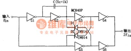
In the figure is the rectangle pulse frequency doubler circuit. This circuit is a digital frequency doubler, which consists of a 6-inverting-phaser MC840P, 2 diodes and a capacitor, and its working frequency is 1Hz~100KHz. The input signal of the circuit is a square wave, and the output is an approximately symmetric rectangle wave. The required capacitive reactance of capacitor C at the frequency is 1kΩ. If the required output is a symmetric square wave, we can connect the capacitor with a resistor in serial or parallel way. The output circuit includes the phase inverters of G3, G4, G5 and G6, and they are coupled by the diodes of D1 and D2. (View)
View full Circuit Diagram | Comments | Reading(840)
The 150-300MHz frequency multiplier composed of MC1596
Published:2011/6/17 20:13:00 Author:Borg | Keyword: frequency multiplier
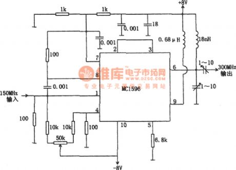
In the figure is the 150-300MHz frequency multiplier. The circuit is made of MC1596 balance modem, whose input frequency is 150MHz and the output frequency is 300MHz. MC1596 has two frequency input terminals(1-pin and 4-pin), and the 150MHZ frequency is added on the two terminals. By adjusting the 50kΩ potentiometer, the two terminals receive the same signal. By adjusting the 2 1~10pF adjustable capacitor, the output frequency will be precisely be twice of the input frequency and the distortion is reduced to the minimum. The input and output impedance are approximate 50Ω. (View)
View full Circuit Diagram | Comments | Reading(1877)
The frequency multiplier composed of XR-S200
Published:2011/6/17 20:14:00 Author:Borg | Keyword: frequency multiplier

View full Circuit Diagram | Comments | Reading(517)
The 3-way frequency circuit of symmetric output(74LS109 and 74LS113)
Published:2011/6/17 20:25:00 Author:Borg | Keyword: 3-way frequency, symmetric output
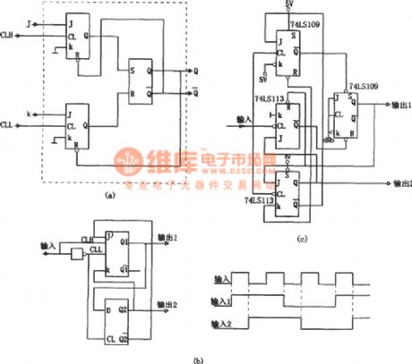
In the figure is the 3-way frequency circuit of symmetric output. Usually, when we use common counter to odd-split the digital pulse, even the input is the symmetric signal, the output won't be the splitting frequency of 50% duty cycle, the reason is that all the internal triggers are motivated by the rising edge (or the dropping edge). To solve the problem, we can use a J and K, two JK triggers that are motivated by the clock, see as figure (a). The circuit includes two JK triggers and a RS trigger. (View)
View full Circuit Diagram | Comments | Reading(1156)
The flash signpost light circuit
Published:2011/6/17 8:05:00 Author:Borg | Keyword: flash signpost light

E.g 7 the flash signpost circuitSee as figure 20-7, the circuit consists of the transforming rectifier circuit, light control switch and non-steady multi-resonance oscillator, etc.The light dependent triode 3DU5 is in a low impedance due to the light in the daytime, which makes the power switch pipe TWH878 block due to the low control voltage of 5-pin, and IC(555) doesn't work without power, SCR is blocked, the light is OFF. The it's dark outside, 3DU5 is in a high impedance without light, which makes the voltage on 5-pin of TWH8778 higher than 1.6v, the switch pipe is conducting, IC is oscillating because of getting power. The oscillating frequency is f=1.44(R2+R3)C2.The frequency responding to the figured parameter is about 1Hz.
(View)
View full Circuit Diagram | Comments | Reading(534)
The continual signal frequency splitting circuit composes of CC4013
Published:2011/6/17 20:40:00 Author:Borg | Keyword: signal frequency, splitting circuit
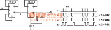
In the figure is the continual signal frequency splitting circuit composes of CC4013. This circuit consists of a double frequency splitter circuit and a single steady circuit, which can fulfill the splitting function with external signals, but when the input signal is halt, the circuit can come back to the 0 state automatically. The single steady time can be adjusted according to requirements. The input signal is in the terms of continual bundles. After it crosses the 1st stage frequency splitter, though the pulse in the bundle is split, the interval between bundles may be in the low LEV (if the number of the pulse in the bundle is even). (View)
View full Circuit Diagram | Comments | Reading(534)
The sine wave frequency-halving circuit (μA747 and μA795)
Published:2011/6/17 20:54:00 Author:Borg | Keyword: sine wave, frequency-halving circuit
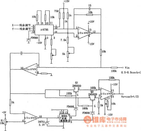
To an ordinary digital frequency splitting circuit, the weakness is that it can't maintain the former sine waveform. If the sine wave output is needed, we can add a additional filter or the like, see as the circuit. In the circuit, the integrated circuits of μA795 and μA747C compose the standard square root circuit. The output of circuit the positive square root of the input voltage absolute value. When the input ±0.5cosωt, the output is cos( ωt/2). The trigger 9094, analog switches (Q1 and Q2) and half of the computing amplifier μA747 consist of the absolute value removing circuit. (View)
View full Circuit Diagram | Comments | Reading(866)
The 10~100MHz frequency splitter composed of MC1013
Published:2011/6/17 21:28:00 Author:Borg | Keyword: frequency splitter
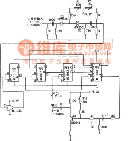
The working frequency of the circuit can reach 100MHz, the heat loading diode limiters (D1 and D2) can transport the 10V signals to the gate circuit MC1023 without any loss. The changeable resistor R1 is the bias point that controls D1 and D2, which makes the positive voltage of D1 be -3.2v. The amplitude limiter outputs a signal that is rectified by the high speed pulse driver MC1023, and the signal is delivered to the 120MHz J-K trigger FF1 and split into two. The output of FE1 is put into the dividing 5 circuits (FF2,FF3 and FF4), then the output drive transistor Q1 of FF4 generates a square wave whose amplitude is 2~4v and frequency is 1~10MHz. (View)
View full Circuit Diagram | Comments | Reading(806)
The 1GHz preset frequency splitter composed of SP6168
Published:2011/6/17 21:39:00 Author:Borg | Keyword: frequency splitter
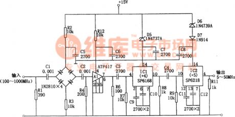
In the figure is the 1GHz preset frequency splitter. The splitter is powered by a +15v single power supply, whose sensitivity is 30mVrms, and it has a dynamic range of 40dB, its working frequency is 100~1000MHz. In the figure, the input signal is coupled to the diode bridge amplitude limiter by the capacitor, the peak value of the limiter output signal is 100mV, which is amplified by the wide frequency calculating amplifier A1, and then coupled to the 4 point frequency circuit by C3. R6 is the output terminal loading of A1, R7 is the input bias resistor of R7. The output is coupled to the 5-point frequency by the capacitor. (View)
View full Circuit Diagram | Comments | Reading(426)
The digit controlled frequency splitter composed of MC4018
Published:2011/6/17 21:50:00 Author:Borg | Keyword: frequency splitter

In the figure is the digit controlled frequency splitter and Figure (a) is the principle circuit. The circuit can set any splitting constant and output a square wave. To a random even number N, the N can be written as N=2M, and to a random odd number, which can be represented as N=2M+1. If N is represented in the binary way, the minimum binary bit may be removed and it gets M, so the frequency splitting constant can be controlled by the binary number. Therefore, to a certain N, we can design a M frequency splitter. For example, if N=181, then the M added on the splitter will be 90. (View)
View full Circuit Diagram | Comments | Reading(526)
The practical ultrasonic remote control circuit
Published:2011/6/19 10:29:00 Author:Seven | Keyword: ultrasonic, remote control

The practical ultrasonic remote control circuit is shown as follows.
figure 1. the emitting circuit (View)
View full Circuit Diagram | Comments | Reading(780)
The STK4171 application circuit
Published:2011/6/19 10:27:00 Author:Seven | Keyword: application circuit

The STK4171 application circuit is shown as follows:
(View)
View full Circuit Diagram | Comments | Reading(3196)
The sensitive frequency demodulator (LM565 and LM111) circuit
Published:2011/6/16 21:21:00 Author:qqtang | Keyword: sensitive frequency demodulator
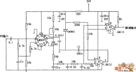
This circuit consists of the phase-lock integrated circuit LM565, which can track the frequency shift in a wide frequency range. However, to the low frequency signal, as the demodulating output signal is weak, the drifting of the voltage control oscillator will cause the drifting of the comparator working point and then cause faults. To overcome the above weakness, we add a DC recover part in the circuit, so it can work stably even when the frequency of the signal is weak. In the figure, the demodulating circuit composed of LM565 and comparator LM111 is almost the same with ordinary frequency demodulator circuits.
(View)
View full Circuit Diagram | Comments | Reading(1211)
The dual-channel output switch stable power supply circuit
Published:2011/6/16 21:28:00 Author:qqtang | Keyword: dual-channel, stable power supply

The dual-channel output switch stable power supply circuit is shown as follows.
(View)
View full Circuit Diagram | Comments | Reading(833)
The PLL FM demodulator (4046) circuit
Published:2011/6/16 21:26:00 Author:qqtang | Keyword: FM demodulator

See as the figure, the FM demodulator (4046) circuit consists of 4046 PLL particles, the intermediate FM input signal is demodulated into the low frequency by the circuit.
(View)
View full Circuit Diagram | Comments | Reading(7129)
The producing circuit of the digit displaying "L and C" meter
Published:2011/6/19 20:06:00 Author:qqtang | Keyword: producing circuit, digit displaying
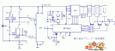
View full Circuit Diagram | Comments | Reading(479)
The 567 FM demodulator circuit
Published:2011/6/16 21:58:00 Author:qqtang | Keyword: FM demodulator circuit


In the figure is the 567 FM demodulator circuit. In the figure, the FM signal is input from 3-pin and the demodulated signal is output from 5-pin. The central frequency of the FM signal that the circuit can demodulate is: fo=1.1/RC. In the circuit, C1 is the filtering capacitor, C2 is the wide band adjusting capacitor, when C2 is going down, the band width of the demodulator is rising. The selecting basis of C2 is:
There is also a demodulation indicating circuit. When the demodulation is right, 8-pin is outputting a low LEV. When the indicator is on, it is glowing, the indicator can also be pick out and used as the control signal.
(View)
View full Circuit Diagram | Comments | Reading(2367)
The vmos switch power steady circuit
Published:2011/6/16 22:00:00 Author:qqtang | Keyword: power steady circuit

View full Circuit Diagram | Comments | Reading(524)
The RX3310A reception module circuit
Published:2011/6/16 22:14:00 Author:qqtang | Keyword: reception module circuit
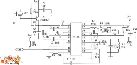
The RX3310A module is a wireless remote control and digit transiting signal reception module which is specially used in amplitude key control ASK modulation. This module is made of high function wireless remote control and digit transiting special integrated circuit, which contains the low-noise high-frequency amplifier, mixer, local oscillator, intermediate frequency amplifier, intermediate frequency filter, comparator and so on, and it is also fixed with the 316.8MHz sound surface wave resonator, so that it works stably and it's fitted to work in bad conditions.The superhet receiving module circuit of RX3310A:
(View)
View full Circuit Diagram | Comments | Reading(1829)
The 5V and 5a switch stable power supply circuit
Published:2011/6/16 22:16:00 Author:qqtang | Keyword: power supply

The 5V and 5a switch stable power supply circuit is shown in the following circuit.
(View)
View full Circuit Diagram | Comments | Reading(640)
| Pages:1745/2234 At 2017411742174317441745174617471748174917501751175217531754175517561757175817591760Under 20 |
Circuit Categories
power supply circuit
Amplifier Circuit
Basic Circuit
LED and Light Circuit
Sensor Circuit
Signal Processing
Electrical Equipment Circuit
Control Circuit
Remote Control Circuit
A/D-D/A Converter Circuit
Audio Circuit
Measuring and Test Circuit
Communication Circuit
Computer-Related Circuit
555 Circuit
Automotive Circuit
Repairing Circuit