
Circuit Diagram
Index 1749
The surrounded sound generator composed of TA8173AP
Published:2011/6/16 0:52:00 Author:Borg | Keyword: surrounded sound, generator

See as the figure, both the output and input are dual-channel, by the switch on 13-pin, we can choose normal sound or surrounded sound. After crossing the buffer, the input R and L signal is split into the main signal and vice signal. The vice signal is sent to the low-pass filter LPFI by R-L, then it shifts the phase, and then it crosses the low-pass filter LPF2 and is added with the main signal by the switch. The R channel signal is to do the same phase addition, so that the signal that we get is sent out by the low-pass filter LPF3 and the buffer. (View)
View full Circuit Diagram | Comments | Reading(1931)
The 100 times frequency circuit composed of CD4046
Published:2011/6/16 5:25:00 Author:Borg | Keyword: frequency, circuit
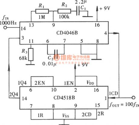
View full Circuit Diagram | Comments | Reading(3746)
The sawtooth wave generating circuit composed of μA741 integrated op-amps
Published:2011/6/16 0:04:00 Author:Borg | Keyword: sawtooth wave, integrated op-amps
View full Circuit Diagram | Comments | Reading(567)
The BH3006 application circuit of the waveform generating integrated circuit
Published:2011/6/16 0:02:00 Author:Borg | Keyword: application circuit, waveform, integrated circuit

View full Circuit Diagram | Comments | Reading(538)
The audio noise generator
Published:2011/6/16 0:18:00 Author:Borg | Keyword: audio noise generator
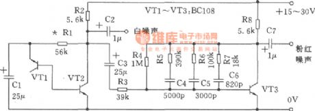
In the figure is a simple circuit which can generate white and pink noises. The voltage steady pipe is the crystal triode VTI, which generates wide-band noises in the Zener breakdown state. After being amplified by VT2, a white noise of 150mV or so is output by capacitor C2. To convert the white noise into pink noise, we use a filter net, each frequency doubler of this filter provides a 3dB reduction. As the filter reduces much of the noise, so we need an amplifier to recover the output LEV. (View)
View full Circuit Diagram | Comments | Reading(1331)
The white noise generator
Published:2011/6/16 0:35:00 Author:Borg | Keyword: noise generator

In the figure is the ICMM5837 wide-band white noise generator, the white noise is generated by the 3dB filter of the 10Hz to 40KHz octave. The noise has flat frequency distribution within 20Hz to 20kHz. The output is added on the 1Vp-p noise on the 8.5v DC LEV. This circuit is mainly used to the controllable noise source. Components selecting: integrated circuit IC: MM5837; capacitor CI:100μ25V,C2:1μ50V,C3:0.27μ63V,C4、C5:0.047/63V,C6:0.033μ63V. Resistor RI: 6.8kΩ,R2:3k,R3:1k,R4:300Ω, all of which are l/8WRJ type.
(View)
View full Circuit Diagram | Comments | Reading(1771)
The video boosting circuit
Published:2011/6/16 0:07:00 Author:Borg | Keyword: boosting circuit
View full Circuit Diagram | Comments | Reading(594)
The frequency synthesizer formed by CD4046
Published:2011/6/16 5:40:00 Author:Borg | Keyword: frequency synthesizer

The so-called frequency synthesis means converting a certain reference frequency ^ into a series of new frequencies like fo1、fo.....fon. These new frequencies have the same stability as the former reference frequency. If we put a frequency splitter, whose splitting constant is fixed, between the 3-pin and 4-pin of CD4046, a new frequency doubler with the fixed multiple is formed. If we insert a multi-stage splitter with adjustable constants, then a multi-stage adjustable doubler is formed, which is the frequency synthesizer . In the figure is a frequency synthesizer made of CD4017. (View)
View full Circuit Diagram | Comments | Reading(6022)
The precise frequency synthesizer composed of CD4046
Published:2011/6/16 5:50:00 Author:Borg | Keyword: frequency synthesizer
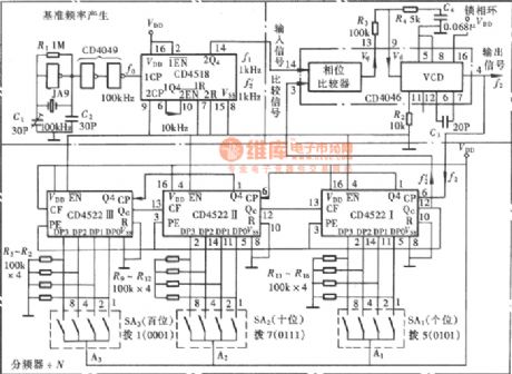
In the figure is a practical frequency synthesizer, which is equipped with a highly stable quartz crystal oscillator, and it generates a 100KHz rectangle pulse which is split into 1KHz pulse by the splitter as the reference frequency. The synthesizer is preset by a switch, which can output 999 kinds of reference frequencies that are 1~999kHz with the interval of 1KHz. The synthesizer is very useful.
(View)
View full Circuit Diagram | Comments | Reading(4169)
High-voltage pulse generator
Published:2011/6/16 5:47:00 Author:Lucas | Keyword: High-voltage, pulse generator

The circuit is shown as the chart, it uses the 6V ~ 12V DC power supply to produce high-voltage pulse. In the circuit, the transistors VTl, VT2 constitute an oscillator to produce a DC pulse voltage with the frequency in 3Hz, and it has the primary coil of booster with the output transformer ratio in 6V: 240V, and after each pulse ends, the secondary coil of corresponding transformer will generate a high voltage level. Pulse repetition frequency can be selected by adjusting C2, Rl. When the circuit is used in the baton, it can use lead-acid batteries.
(View)
View full Circuit Diagram | Comments | Reading(51)
White LED drive circuit composed of TL499A
Published:2011/6/13 6:16:00 Author:Lucas | Keyword: White LED, drive circuit
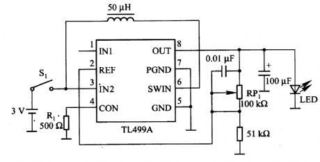
Figure 2-12 shows the white LED drive circuit which is composed of the TM499A. The white LED driver voltage is about 3.6 V. If it uses an ordinary battery to supply power, you need the step-up circuit, and it uses the boost circuit composed of the TL499A. TL499A is an integrated regulator with adjustable output voltage, and when it boosts, it needs switching regulator mode, and when it bucks, it needs the linear regulator mode. The two working modes can change automatically according to the input voltage. Input voltage range is 1.1 10V (switching work), and the maximum voltage is 35V (linear regulator work); the output voltage range is 2.9 to 30V, the maximum output current is 100mA. In the figure, the working power supply is supplied by 1- 2 batteries which are connected in series, and Ip is the controlling peak switch current of pin 4 in TL499A, and when Rl is 5OOΩ, Ip is about 2OOmA.
(View)
View full Circuit Diagram | Comments | Reading(2122)
MC3425 over power monitoring circuit, voltage regulator
Published:2011/6/14 4:42:00 Author:Lucas | Keyword: over power , monitoring circuit, voltage regulator
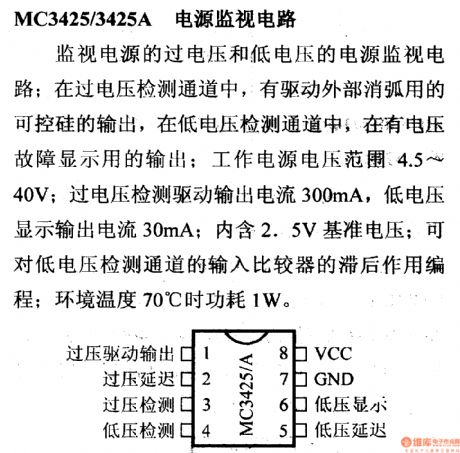
MC3425 over power monitoring circuit, voltage regulator, DC-DC circuit, pin and features of PWU
It is the power monitoring circuit with over-voltage and low voltage; in over-voltage detection channel, there is the external SCR output which is used to drive external arc extinction; in the low-voltage detection channel, there is a display with the output voltage failure; the work voltage range is 4.4 ~ 40V; the over-voltage detection driver output current is 300mA, and low voltage display output current is 30mA;the inter includes 2.5V reference voltage, which can do the programming on the hysteresis of input comparator in the low voltage detection channel, and when the temperature is at 70 ℃, the power consumption is 1w.
(View)
View full Circuit Diagram | Comments | Reading(455)
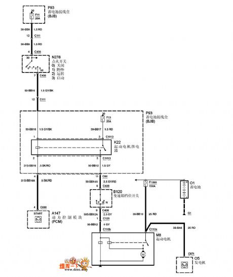
Ford Focus automatic gear-box circuit
Published:2011/6/11 1:38:00 Author:chopper | Keyword: Ford Focus, automatic, gear-box
View full Circuit Diagram | Comments | Reading(674)
CNY44 analog isolation circuit
Published:2011/6/11 1:37:00 Author:chopper | Keyword: analog, isolation

This circuit can be used when the analog signals is transmitted among equipment of different earth potential.The 3 dB bandwidth of the circuit is between 6HZ and 80KHZ,and between 100KHZ and 20KHZ,the total harmonic distortion is less than 1.5% when +8V(peak-peak) outputs power Level.
(View)
View full Circuit Diagram | Comments | Reading(1542)
The sine wave generating circuit
Published:2011/6/16 6:03:00 Author:Seven | Keyword: sine wave, generating

View full Circuit Diagram | Comments | Reading(723)
The half-wave rectifier circuit-single phase half-wave rectifier circuit
Published:2011/6/16 6:01:00 Author:Seven | Keyword: half-wave rectifier
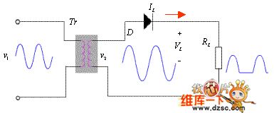

The half-wave rectifier is a motor that uses the single conducting way feature of the diode, and makes half of the voltage V0 from the transformer reach the load, finally makes the loading voltage VL be a single way pulse DC voltage.
 Main parameters:
(View)
Main parameters:
(View)
View full Circuit Diagram | Comments | Reading(1031)
The oscillating circuit composed of crystal and NOR gate
Published:2011/6/16 6:17:00 Author:qqtang | Keyword: oscillating circuit, NOR gate

In the figure is the oscillating circuit composed of crystal and NOT gate. In the circuit, X is the 1MHz crystal, and it connects with 10 frequency splitting circuits, which has 6 stages of parallel connections. Therefore, it can pick out signals of different frequencies from different output terminals, i.e A terminal outputs 100KHz frequency, B outputs 10KHz, C outputs 1KHz, D outputs 100 Hz, E outputs 10Hz, F outputs 1Hz and so on.
(View)
View full Circuit Diagram | Comments | Reading(711)
The frequency doubler circuit of high but few harmonic waves
Published:2011/6/16 6:29:00 Author:qqtang | Keyword: frequency doubler, harmonic waves
In the figure is the frequency doubler circuit of high but few harmonic waves. When the high frequency signal can'T be got from the crystal circuit directly, this circuit can be fixed in the oscillating circuit and high frequency signals can be got. As there is a modulation circuit, the frequency band turns narrow, but the high frequency output signals are pure. When the input is -2dBm, an output voltage of 6dBm can be got, the distortion of the high frequency harmonic wave is lower than -6dB.
(View)
View full Circuit Diagram | Comments | Reading(835)
The 60Hz time-based generator composed of MM5369
Published:2011/6/15 21:23:00 Author:Borg | Keyword: time-based generator
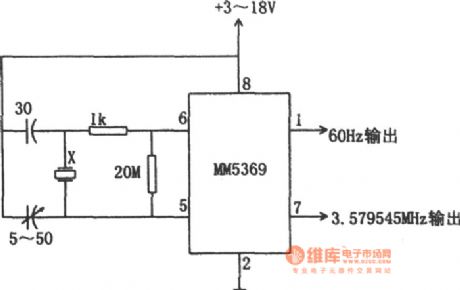
In the figure is the 60Hz time-based generator composed of MM5369. In many conditions, 60Hz has been a reference frequency, such as electric clock, timer and controller, etc, and all of their reference frequencies are 60Hz. So a independent 60Hz signal source is often in need, which is used in portable or battery power supplies for test or development. This circuit is formed by the integrated TV MM5369 time-based generator. The device needs external crystal which is cut according to the standard color synchronized signal frequency of standard 3.57954MHz. (View)
View full Circuit Diagram | Comments | Reading(3550)
555 TV starting up timer circuit
Published:2011/6/15 3:34:00 Author:TaoXi | Keyword: 555, TV, starting up, timer circuit


As the figure 14-13 shows, the timer is composed of the benchmark pulse generator, the reservation time limit interlock switch, the counter and the driving circuit. And this device can be used to control the children watching TV time. The time limit has five levels: the limit time of K1 is 40 minutes, the locking time is 280 minutes; the limit time of K2 is 80minutes, the locking time is 240 minutes; the limit time of K3 is 160 minutes, the locking time is 160 minutes; the limit time of K4 is 280 minutes, the locking time is 40 minutes; if you do not press K1~K4, the limit time is 320 minutes.
The astable oscillator is composed of the IC1 (555) and R1, RP1, C1, the oscillation period T=0.693(R1+RP1)C1, the T of the figure parameter is about 40 minutes. The output of it can be used as the count pulse of the counting circuit IC2.
(View)
View full Circuit Diagram | Comments | Reading(1026)
| Pages:1749/2234 At 2017411742174317441745174617471748174917501751175217531754175517561757175817591760Under 20 |
Circuit Categories
power supply circuit
Amplifier Circuit
Basic Circuit
LED and Light Circuit
Sensor Circuit
Signal Processing
Electrical Equipment Circuit
Control Circuit
Remote Control Circuit
A/D-D/A Converter Circuit
Audio Circuit
Measuring and Test Circuit
Communication Circuit
Computer-Related Circuit
555 Circuit
Automotive Circuit
Repairing Circuit