
Circuit Diagram
Index 1750
555 TV square grid generator circuit
Published:2011/6/15 3:58:00 Author:TaoXi | Keyword: 555, TV, square grid, generator circuit
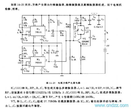
As the figure 14-20 shows, the square grid generator is composed of the line frequency oscillator, the field frequency oscillator and the high frequency oscillator, it can be used in the overhaul and calibration of the TVs.
The astable multivibrator is composed of the IC1(555) and R1, RP1, R3, C1, the f1=1.44/(R1+RP1+2R3)C1, by adjusting RP1, we can make the oscillation frequency on the 125kHz which is 8 times of the line frequency; the multivibrator is composed of the IC2(555) and R6, RP2, R8, C4, the f2=1.44/(R6+RP2+2R8)C4, by adjusting RP2, we can make the oscillation frequency on the 300kHz which is 6 times of the line frequency.
The 57.75MHz wave-carrier oscillator is composed of the VT1 and L1, C7, C8, C12, it is adjusted by the output pulses of IC1 and IC2, and it radiates by the L1, C7 oscillation loop.
(View)
View full Circuit Diagram | Comments | Reading(1019)
555 electronic musical instrument additional combo audio circuit
Published:2011/6/15 4:22:00 Author:TaoXi | Keyword: 555, electronic musical instrument, additional, combo audio circuit
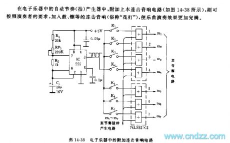
If we add this combo audio circuit (as the figure 14-38 shows) to the automatic rhythm generator of the electronic musical instruments, we can meet the the requirements of players to add the combo audio of drum and cymbals to make the performance effect more perfect.
As the figure shows, the astable multivibrator is composed of the 555 and R1, RP1, R2, C1, the oscillation period T=0.693(R1+RP1+2R2)C1, the oscillation period sound effects are adjustable. If you press different K(K1~K7), you can get the corresponding combo sound. By adjusting RP1, you can change the frequency of the combo sound.
(View)
View full Circuit Diagram | Comments | Reading(1648)
555 multi-function sound generator
Published:2011/6/15 4:58:00 Author:TaoXi | Keyword: 555, multi-function, sound generator
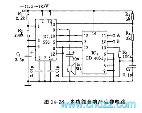
As the figure 14-28 shows, the sound generating circuit is composed of the 556 and CD4051, this circuit can produce the single, dual-tone and rhythm-style sound.
The astable oscillator is composed of the IC's left part (1/2 556) and R1, R2, C1, f=1.44/(R1+2R2)C1, the oscillation frequency of the figure parameter is 2Hz, it's output port pin-5 is connected with the public input / output port (pin-3) of IC2, IC2 is the 8-channel analog switch CD4051, the port A and port B control one channel's connection of this switch.
The sound oscillator is composed of the IC1(1/2 556) and the R3, R4, C2. When A=0,B=0, this circuit outputs the double audio frequencies sound signal; when A=1,B=1, the 2Hz signal which is produced by the left part of IC1 does not play the control function until it outputs the single-tone with the frequency of 900Hz.
(View)
View full Circuit Diagram | Comments | Reading(2153)
555 multi-function analog audio circuit
Published:2011/6/15 6:45:00 Author:TaoXi | Keyword: 555, multi-function, analog, audio
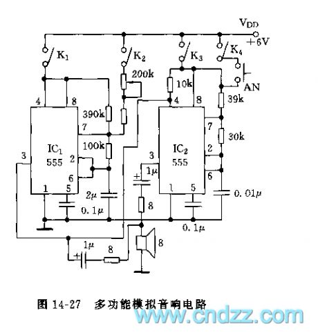
As the figure 14-27 shows, the multivibrator which is composed of two bipolar type 555s (or a 556) and the capacitance resistance elements can form a variety kinds of analog audio circuits. The oscillation frequency of IC1 is about 1Hz, the duty ratio is about 80%. The oscillation frequency of IC2 is about 1500Hz. By using the opening and closing of the switch, this circuit can simulate different sounds. For example, when you just turn on the K1, the IC1 starts working, the circuit will send out the monotonous second signal; if you just turn on the K4, the IC2 starts working, the circuit will send out the 1500Hz alarm signal; if you turn on the K3 and K4 at the same time, you can realize the modulation of IC1 to IC2, the circuit will send out the intermittently sound.
(View)
View full Circuit Diagram | Comments | Reading(667)
555 multi-stage electronic metronome circuit
Published:2011/6/15 7:02:00 Author:TaoXi | Keyword: 555, multi-stage, electronic metronome
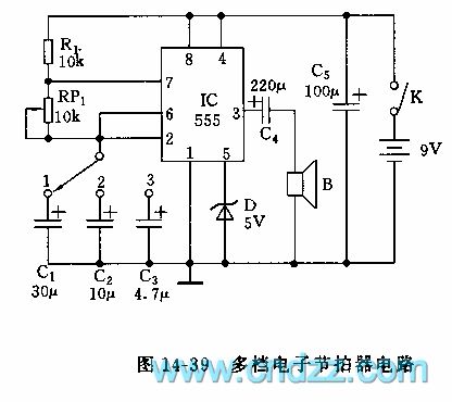
As the figure 14-39 shows, in this circuit the 555 is used as the astable multivibrator. The circuit beat is divided into three stages to be controlled, the oscillation frequency f1=1.44/(R1+RP1)C1, it is about 20-60 beats/min; f2=1.44/(R1+RP1)C2, it is about 60-80 beats/min; f3=1.44/(R1+RP1)C3, it is about 180-540 beats/min; after you know the calculation formula, you can change the charging and discharging time constant RC by yourself according to the actual situation to adjust the frequency or the beat. Also you can increase or decrease the number of stages. In order to make the beat more accurate and the parameters more stable, you need to use the metal film RJ as the resistance, and the electrolytic capacitor need to have the features of small leakage of electricity and high voltage capacitance.
(View)
View full Circuit Diagram | Comments | Reading(1614)
555 audio signal array display circuit
Published:2011/6/15 7:19:00 Author:TaoXi | Keyword: 555, audio signal, array display
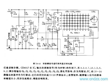
This circuit is composed of the audio signal amplification circuit, the pulse position modulation circuit, the counting circuit, the audio display driver stage array circuit.etc. As the figure 14-44 shows.
The input audio signal adds to the input port pin-8 of IC3(TBA810) through the electrical level adjustment potentiometer RP1. The output amplified signal is divided into two channels, one channel adds to the pin-3 of audio display driver stage IC1(LB1405), another channel adds to the voltage control port pin-5 of the IC4(555) time-base circuit as the pulse position modulation mode sync signal. When there is no input signal, the resonance frequency of 555 is f0=1.44/(R11+2R12+RP2)C11. The resonance frequency of the parameters is 59~61Hz, by adjusting RP2, you can make the resonance in the center frequency f0=60Hz.
(View)
View full Circuit Diagram | Comments | Reading(1868)
555 autoplay radio gymnastics record device circuit
Published:2011/6/14 3:52:00 Author:TaoXi | Keyword: 555, autoplay, radio gymnastics, record device
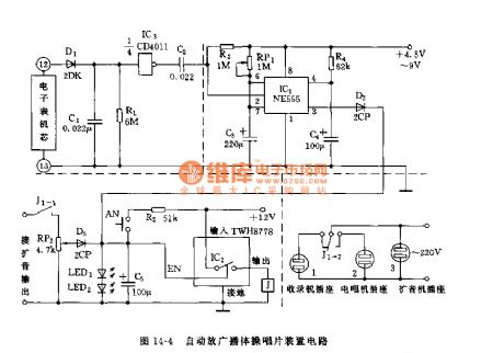
As the figure 14-4 shows, this device is composed of the electronic watch timer, the monostable circuit, the delay amplitude discriminator circuit.etc. And this device can be used to timing play the radio gymnastics record every day.
The timing signal is from the pin-12 and pin-13 of the electronic watch, when the electronic watch jumps from the 11:P to 12:A, the IC3(1/4CD4011) outputs a negative pulse transition to trigger the monostable timing circuit which composed of the 555 and RP1, C3, the timing time td=1.1RP1C3, the figure parameters' maximum delay is about 8 minutes.
The amplitude discriminator which is composed of the C5, TWH8778, LED1, LED2, J has the delay function, J1-2(left) is the contact-point of the normally closed relay, when the radio socket has the electricity, the radio starts working.
Figure 14-4 The 555 autoplay radio gymnastics record device circuit (View)
View full Circuit Diagram | Comments | Reading(789)
555 automatic radio controller circuit
Published:2011/6/14 4:05:00 Author:TaoXi | Keyword: automatic, radio controller

As the figure 14-5 shows, this controller can be used to control the electronic valve audio power amplifier.
When the clock control system connected to the trigger switch S, J1 closes, the power turns on. The boot delay circuit is composed of the IC2 and R2, C3, the delay time td1=1.1R2C3, it is about 2-5 minutes, then the J2 closes to connect the high voltage. The ten minutes delay circuit is composed of the IC2 and C8, R5, if there is no monitor signal in ten minutes, the pin-3 will output the high electrical level to supply power to the IC3, and IC3 outputs the high electrical level to close J3, the high voltage turns off. The monostable delay circuit is composed of the IC3 and C9, RP3, R8, the delay time td2=1.1(R8+RP3)C9, it is about 10 seconds.
(View)
View full Circuit Diagram | Comments | Reading(491)
555 synchronization/quasi-synchronization video-audio switching circuit
Published:2011/6/14 6:19:00 Author:TaoXi | Keyword: 555, synchronization, quasi-synchronization, video-audio, switching

As the figure 14-19 shows, this circuit is composed of the improved R-S bistable trigger circuit (composed of the 555) and the four-analog switch CD4066. This circuit has the function of synchronous switching and quasi-synchronous switching.
The NAND gate is composed of the VT1 and VT2, the OR gate is composed of the VT3 and VT4, they control the IC1(555)'s trigger port (pin-2) and the reset port (pin-4) respectively, VT6 is the set lock circuit. The connection method of this circuit makes the video input I and the audio input I to be the priority channel, that is why the VT1 and VT4 are in the cut-off state. When you need to input I, you should press AN1, the VT2 conducts, the pin-2 of 555 has the low electrical level to lock the set state.
(View)
View full Circuit Diagram | Comments | Reading(646)
555 radio digital frequency displayer circuit
Published:2011/6/14 6:38:00 Author:TaoXi | Keyword: 555, radio, digital, frequency displayer, circuit
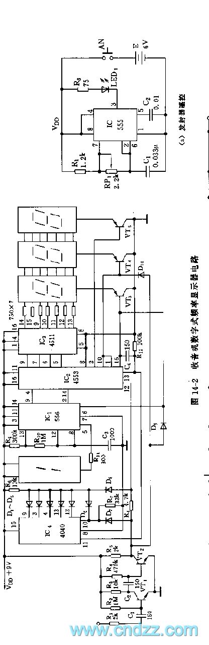
As the figure 14-2 shows, this circuit is composed of four pieces of integrated circuits and four LED luminescence digital tubes to display the frequency of the medium-wave station, it displays the frequency accurately and the circuit is simple.IC1 uses the dual time-base circuit 556, the astable multivibrator is composed of the 1/2 556 and the R9, R10, C3, the oscillation frequency f=1.44/(R9+2R10)C3, it is about 1000Hz, the output of pin-9 adds to IC2's external scanning input port pin-4. Another half of 556 (1/2 556) is connected as the trigger, the output of pin-5 adds to the luminescence digital tube.
The IC2(MC14553) is a BCD code 3-bit counter. The AND gate is composed of the D9 and D10. When the pin-1 and pin-15 have the low electrical level, the VT3 and VT4 conduct.
(View)
View full Circuit Diagram | Comments | Reading(601)
555 radio wireless remote control switch additional device circuit
Published:2011/6/14 6:57:00 Author:TaoXi | Keyword: 555, radio, wireless, remote control, switch, additional device

As the figure 14-1 shows, this additional device has a medium-wave amplitude modulation transmitter and a tape recorder additional circuit. When you are remote controlling, this device will launch a short amplitude modulation pulse (<1 second), so the remote control switch turns on; if it launches a long pulse (>2 second), the remote control switch turns on to remote control all sorts of home appliances, the effective distance is 6-12 meters.
The audio oscillator is composed of the VT1 and R1,C1,T1, the high-frequency oscillator is composed of the VT2 and T2, C2, C4, R2 to send out the audio modulation high frequency pulse signal, the pulse width depends on the press-time of AN1.
(View)
View full Circuit Diagram | Comments | Reading(1906)
555 radio automatic sentence spliting playback circuit
Published:2011/6/14 7:22:00 Author:TaoXi | Keyword: 555, radio, automatic, sentence spliting, playback circuit
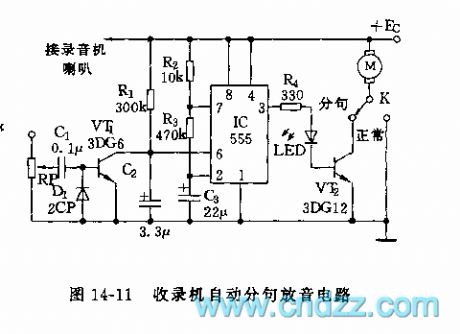
When there is the playback signal, the signal is rectified by D1 to conduct the VT1, and C2 discharges. The 555 is in the set state, the LED turns on, the VT2 conducts, the motor M starts working to send out the sound. When sentence is over, the VT1 cuts off, the C2 is charged by R1, after about 1 second, when the voltage of C2 is higher than the threshold level 2/3VDD, the 555 resets to output the low electrical level, the M stops working. At the same time, the C3 discharges to the disrharge tube of 555 substrate through R3, when the voltage of C3 is lower than 1/3VDD, the 555 sets again, pin-3 has the high electrical level, M stops working. The discharging time tdischarge=1.1R3C3, the tdischarge of the figure parameters is about 10 seconds for the follow reading.
(View)
View full Circuit Diagram | Comments | Reading(433)
555 four octaves tone generator circuit
Published:2011/6/14 7:47:00 Author:TaoXi | Keyword: 555, four octaves, tone generator
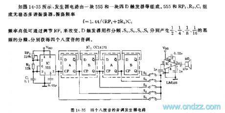
As the figure 14-35 shows, the generator circuit is composed of one piece of 555 and a four-D trigger. The astable multivibrator is composed of the 555 and RP1, R2, C1, the oscillation frequency f=1.44/(RP1+2R2)C1, the frequency can be changed by adjusting the RP1. The trigger D can be used as the frequency divider, S2,S3,S4 and S5 produce the 1/2,1/4,1/8 and 1/16 frequency divisions of the fundamental frequency, so we get four octave tones.
Figure 14-35 The555 four octaves tone generator circuit (View)
View full Circuit Diagram | Comments | Reading(879)
555 infrared remote control eight-channel selection radio circuit
Published:2011/6/14 8:18:00 Author:TaoXi | Keyword: 555, infrared remote control, eight-channel selection, radio
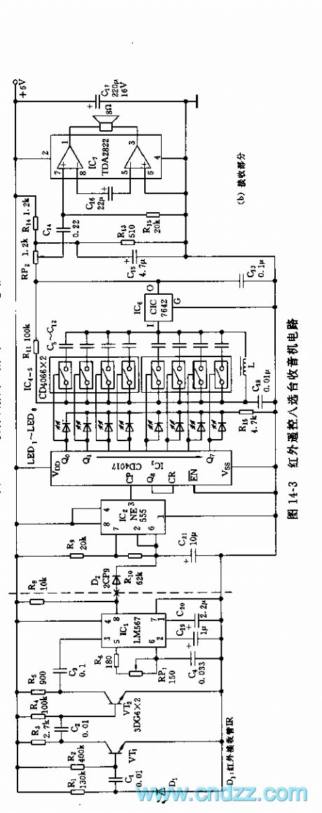
As the figure 14-3 shows, the infrared remote control eight channels radio circuit is composed of the infrared remote control transmitter, the remote control decoder and the channel selection recording part.The remote transmitter is composed of the multivibrator (composed of the 555 and R1, RP1, C1) and the infrared transmitting tube, the oscillation frequency f=1.44/(R1+RP1)C1, the frequency of the figure parameters is about 120kHz, the duty ratio is 67%.
The receiving part is composed of the infrared receiving amplifier, the decoding circuit IC1, the pulse distribution circuit, the electronic switch selective passing radio circuit and the amplifier stage. D1 is the receiving tube which can be used with the launch infrared diode, the VT1 and VT2 are the signal amplification stage. The IC1 uses the PLL audio decoder LM567.
The monostable trigger circuit is composed of the IC2(555) and R9, R10, C21, this circuit outputs the pulse with 1 second pulse width.
(View)
View full Circuit Diagram | Comments | Reading(630)
555 point-frequency TV terminal circuit
Published:2011/6/14 20:28:00 Author:TaoXi | Keyword: 555, point-frequency, TV, terminal circuit

As the figure 14-17 shows, this circuit is composed of the input circuit, the line frequency synchronization generator, the sample-and-hold circuit, the voltage control delay generator and the RF modulator.
The input circuit is composed of the input attenuator RP1 and the emitter follower VT1. The astable multivibrator is composed of the IC2 (555) and RP2, C4.etc, by adjusting RP2, you can make the IC2 to output the pulse waveform which is synchronous as the line scanning frequency 15625Hz, and this pulse is output by pin-3 to add to the trigger port pin-2 of IC1 as the sampling pulse, at last it adds to the e pole of the RF modulator VT2. The sampling and voltage control delay pulse generator is composed of the IC2 (555) and R5, R6, C2.etc.
(View)
View full Circuit Diagram | Comments | Reading(1498)
555 TV double-channel monitoring automatic conversion circuit
Published:2011/6/15 2:19:00 Author:TaoXi | Keyword: 555, TV, double-channel, monitoring, automatic conversion

As the figure 14-14 shows, the conversion circuit is composed of the high duty ratio square-wave generator and the electronic switch, it can be used in the automatic conversion of the two TV channels.
The astable multivibrator is composed of the 555 and R1, R2, C1, because the R1>>R2, so the duty ratio is 99%. The IC2 is the six-inverter CD4069. The IC3 which can be used as the inverter phase control electronic switching circuit of the two channels uses the 4-channel analog switch CD4066. It divides the switches into two groups, one group controls the power supply voltage A1 and tuning voltage B1 of the main channel; another group controls the power supply voltage A2 and the tuning voltage B2 of the monitor channel. K is the 2X2 switch that can be used to select the main and auxiliary channels.
(View)
View full Circuit Diagram | Comments | Reading(803)
The connector circuit of the Hall switch integrated sensor
Published:2011/6/11 22:39:00 Author:qqtang | Keyword: connector circuit, Hall switch integrated sensor
The output voltage and the external magnetic power of the Hall switch integrated sensor are in the linear ratio relationship. This kind of sensors usually consists of Hall parts and amplifiers. When there is an external field, the Hall part is generating a Hall voltage which is in linear relationship with the field power, the voltage is output after being magnified by the amplifier. In the practical circuit designing, to improve the funciton of the sensor, there is always a voltage steady circuit, a current amplifying output stage, a dysfunction adjusting circuit and a linearity adjusting circuit, etc.
(View)
View full Circuit Diagram | Comments | Reading(438)
The the working feature curve circuit of the dual stable state Hall switch integrated sensor
Published:2011/6/11 22:28:00 Author:qqtang | Keyword: working feature curve, stable state, Hall switch integrated sensor
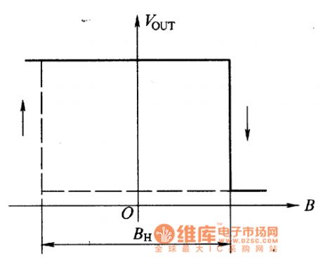
SL3075 Hall switch integrated sensor is a dual stable state sensor, which is also called lock-key sensor, its working feature curve is shown in the figure. When the external magnetic field power is over the working point, the output is in the conducting state. And when the magnetic field is disappearing, the output remains the same, if we want to cut off the output, we should impose an inverting field.
Figure: The the working feature curve of the dual stable state Hall switch integrated sensor (View)
View full Circuit Diagram | Comments | Reading(428)
The working character curve circuit of the Hall switch integrated sensor
Published:2011/6/11 22:21:00 Author:qqtang | Keyword: working character curve, Hall switch integrated sensor
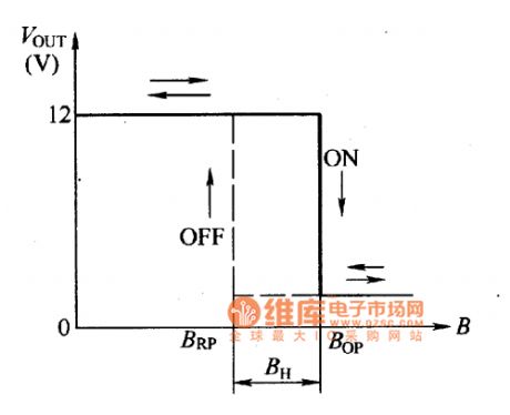
The working character of the Hall switch integrated sensorThe working character of the Hall switch integrated sensor is shown in the figure. Seeing from the working character curve, the working character is with certain magnetic lag (BH), which is good for the reliability of the switch action. In the firgure, Bop is the magnetic sensing power at the working point ON , the RBP is the power of the releasing point OFF .The working character curve of the Hall sensor indicates the relationship between the external magnetic field and the sensor output LEV.
Figure: The working character curve of the Hall switch integrated sensor (View)
View full Circuit Diagram | Comments | Reading(434)
The outline and typical application circuit of the Hall switch integrated sensor
Published:2011/6/11 22:06:00 Author:qqtang | Keyword: typical application circuit, Hall switch integrated sensor
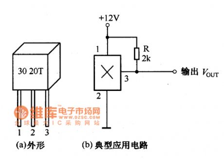
The outline and typical application circuit of the Hall switch integrated sensor are shown in the figure.
figure:The outline and typical application circuit of the Hall switch integrated sensor (View)
View full Circuit Diagram | Comments | Reading(436)
| Pages:1750/2234 At 2017411742174317441745174617471748174917501751175217531754175517561757175817591760Under 20 |
Circuit Categories
power supply circuit
Amplifier Circuit
Basic Circuit
LED and Light Circuit
Sensor Circuit
Signal Processing
Electrical Equipment Circuit
Control Circuit
Remote Control Circuit
A/D-D/A Converter Circuit
Audio Circuit
Measuring and Test Circuit
Communication Circuit
Computer-Related Circuit
555 Circuit
Automotive Circuit
Repairing Circuit