
Circuit Diagram
Index 1616
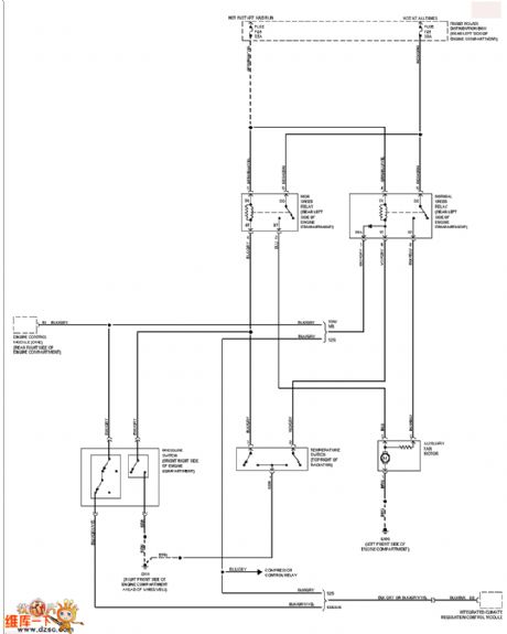
BMW auxiliary air conditioning fan circuit
Published:2011/7/5 21:01:00 Author:Christina | Keyword: BMW, auxiliary, air conditioning fan
View full Circuit Diagram | Comments | Reading(549)
MAX882 linear regulator, main features and pin of DC-DC circuit and power supply monitor
Published:2011/6/30 6:06:00 Author:Lucas | Keyword: linear regulator, main features , pin , DC-DC , power supply monitor


MAX882/ MAX883/MAX884 linear regulator
Output current is 200mA. Input voltage range is 2.7 ~ 11.5V. Output voltage is 3.3V (MAX882 / MAX883) and 5V (MAX884) or adjustable between 1.25 ~ 11V. The voltage will be 200mV when the current is 220mA. Quiescent current is 1 μA, standby mode current is 7μA. It has overload protection function.
(View)
View full Circuit Diagram | Comments | Reading(640)
Electronic transformer circuit diagram
Published:2011/6/30 2:39:00 Author:Ecco | Keyword: Electronic , transformer

The working principle of electronic transformer is the same with the switching power supply, and it is shown in Figure 1 (click to download the schematic). The VD1-VD4 can recify the electric supply to DC, then DC is changed into tens of kilohertz high-frequency current, which is bucked by ferrite transformer. The R2, C1, VD5 in the figure are start trigger circuit. C2, C3, L1, L2, L3, VT1, VT2 constitute the part of high-frequency oscillation.
(View)
View full Circuit Diagram | Comments | Reading(8167)
Complementary symmetry power amplifier circuit diagram
Published:2011/6/30 22:40:00 Author:Ecco | Keyword: Complementary , symmetry, power amplifier

View full Circuit Diagram | Comments | Reading(1850)
The interface circuit diagram of pressure transmitter
Published:2011/7/1 1:38:00 Author:Ecco | Keyword: interface , pressure transmitter

The interface circuit between typical pressure transmitter (such as the Dynisco company's 800 series of pressure transducer) and 1B31 is shown as the chart. 1B31 outputs stable +10 V excitation voltage, and the pressure transmitter full scale output voltage is 30mV. Seting 1B31 gain is 333.3 times could make the 0 to 10,000 lb / inch 2 pressure change into 0 ~ 10V output. For eliminating ground loops, signal returning side and shielded cables must be grounded in the same point. S is the calibration switch, and R is the branch calibration resistor, which can correct full scale output in 80%.
(View)
View full Circuit Diagram | Comments | Reading(1569)
Maintenance circuit diagram of Quartz lamp circuit
Published:2011/7/1 2:57:00 Author:Ecco | Keyword: Maintenance , Quartz lamp

Quartz lamp is widely used in various indoor places of decorative lighting with the advantages of high brightness, condenser, beautiful luxurious, easy installation, low loss, high efficiency. The final stage of the circuit is a buck converter circuit transformer. 220V AC is rectified and inverted to generate about 30kHz ~ 40kHz, 12V AC to light quartz lamp (physical mapping circuit is seen as photo). T is the oscillator output transformer.
(View)
View full Circuit Diagram | Comments | Reading(1071)
(Four-state) touching dimmer control circuit diagram
Published:2011/6/30 22:30:00 Author:Ecco | Keyword: Four-state , touching , dimmer control
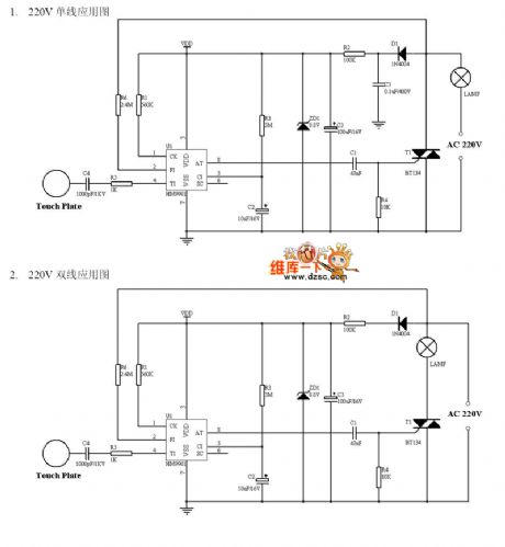
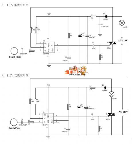
1. 220V mongline application diagram; 2.220V double-line application diagram; 3.110V mongline application diagram; 4. 110V dual-line application diagram
(View)
View full Circuit Diagram | Comments | Reading(1513)
MJE13005 2 electronic ballast circuit diagram
Published:2011/7/1 1:49:00 Author:Ecco | Keyword: electronic ballast

View full Circuit Diagram | Comments | Reading(5745)
100W VMOS FET inverter power supply circuit diagram
Published:2011/7/1 1:27:00 Author:Ecco | Keyword: 100W , VMOS, FET , inverter

Working principle is shown in Figure 1 (click to download the schematic). VT1 and VT2 constitute a multivibrator oscillator with the oscillation frequency in 5Hz. When the voltage drops, the oscillator is provided by the regulator VD1 to keep the same frequency. Multivibrator outputs square wave voltage to drive VMOS high-power tube directly, then the 220V AC is led from the outlet CZ after boosted by step-up transformer. Relay J1 is used for automatical convertion in charging and inverter. LED1 indicates the end of the charging, LED2 is discharged instruction.
(View)
View full Circuit Diagram | Comments | Reading(2142)
MB3756 multiple output regulator, main features and pin of DC-DC circuit and power supply monitor
Published:2011/6/30 20:05:00 Author:Lucas | Keyword: multiple output , regulator, main features , pin, DC-DC , power supply monitor

Three ways of output regulator with fixed output voltage; output voltage is 8.2V; VOUTO and VOUT1 output current is 0 ~ 100mA, VOUT2 output current is 0 ~ 250mA; output voltage range is 11 ~ 16V; VOUT1 and VOUT2 output can achieve noise-free switching by external control signal; Operating Temperature is -20 ~ +75 ℃; it includes overload current and over temperature protection circuit.
(View)
View full Circuit Diagram | Comments | Reading(812)
MB3769 switch control circuit, main features and pin of DC-DC circuit and power supply monitor
Published:2011/6/30 5:49:00 Author:Lucas | Keyword: switch control main features , pin , DC-DC , power supply , monitor


MB3769 switching regulator control circuit It's the switching regulator control circuit with fixed frequency; output is very suitable for power MOS FET-driven totem-pole form; supply voltage range is 12 ~ 18V; the driven load capacity is ± 100mA, ± 600mA; work frequency range is 1 ~ 500KHZ, power is 1000mW; the operating temperature of dual in-line package is -20 ~ +85 ℃, micro-encapsulation is -20 ~ +75 ℃; it includes reference voltage source, which is adjustable dead-time to prevent double pulse; it contains a low voltage power supply circuit to prevent malfunction, stop output during over-voltage.
(View)
View full Circuit Diagram | Comments | Reading(964)
MB3773 power supply voltage monitoring circuit, main features and pin of DC-DC circuit
Published:2011/6/28 5:56:00 Author:Lucas | Keyword: power supply , voltage monitoring , main features , pin , DC-DC circuit

MB3773 power supply voltage monitoring circuit
The instantaneous disconnecting and decreasing of supply voltage will generate the reset signal, when the reset being normal will produce power supply turn-on reset signal, and detection voltage has hysteresis; it has reference voltage output end, and the reference voltage is 1.245V, and error is ± 1.5%; T is the power supply with the limit in -0.3 ~ +20 V; when the ambient temperature is less than 85 ℃, the power consumption is 200mW; Operating Temperature is -40 ~ +85 ℃; it contains edge-triggered input monitoring timer.
(View)
View full Circuit Diagram | Comments | Reading(509)
MB3775 control circuit, main features and pin of DC-DC circuit and power supply monitor
Published:2011/6/28 5:44:00 Author:Lucas | Keyword: control circuit, main features , pin , DC-DC , power supply monitor
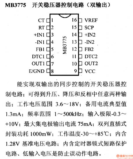
MB3775 switching regulator control circuit (dual output) It is the switching regulator control circuit which can achieve a dual-output synchronous control; it can output boost, buck in inverting way, and the working voltage range is 3.6 ~ 18V; the spare typical current is 1.3mA; frequency range is 1 ~ 500kHz; input limit is -0.3 ~ +10 V; maximum collector output current is 75mA; dual in-line package power is 1000mW; Operating Temperature is -30 ~ +85 ℃; it contains 1.28V reference voltage circuit; it includes timer locking short protection circuit to prevent malfunction circuit from the low input voltage.
(View)
View full Circuit Diagram | Comments | Reading(651)
MB3778 control circuit, main features and pin of DC-DC circuit and power supply monitor
Published:2011/6/22 6:48:00 Author:Lucas | Keyword: control circuit, main features , pin , DC-DC circuit , power supply monitor

MB3778 switching regulator control circuit (dual output) The working supply voltage range is 3.6 ~ 18V; Current consumption is 1.7mA; frequency range is 1 ~ 500 KHZ; error amplifier input limit is -0.3 ~ +10 V; control input (CTL end) limit is -0.3 ~ +20 V; Collector output voltage is 20V; maximum collector output current is 75mA; power cost of dual in-line package is 1000mW; Operating Temperature is -30 ~ 85 ℃; the circuit includes timing, lock short-circuit protection circuit, input voltage malfunction prevention circuit; and it can adjust the rest time in the scope of the whole duty; it has the standby function.
(View)
View full Circuit Diagram | Comments | Reading(506)
MC1403 voltage circuit, main features and pin of DC-DC circuit and power supply monitor
Published:2011/6/22 6:22:00 Author:Lucas | Keyword: voltage circuit, main features , pin , DC-DC circuit , power supply monitor
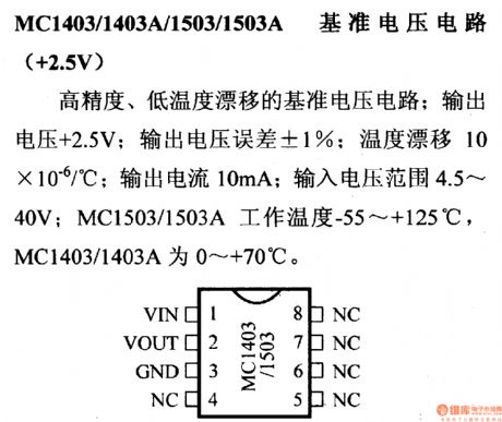
MC1403/1403A/1503/1503A voltage reference voltage circuit(+2.5 V) It's a high-precision, low temperature-drift reference voltage circuit; output voltage is +2.5 V; output voltage error is ± 1%; temperature drift is 10 × 0.000001 / ℃; output current is 10mA ; input voltage range is 4.5 ~ 40V; MC1503/1503A Operating Temperature is -55 ~ +125 ℃, MC1403/1403A is 0 ~ +70 ℃. (View)
View full Circuit Diagram | Comments | Reading(690)
MC1404 voltage circuit, main features and pin of DC-DC circuit and power supply monitor
Published:2011/6/22 6:28:00 Author:Lucas | Keyword: voltage circuit, main features , pin , DC-DC circuit , power supply monitor


MC1404/1404A/1504 voltage reference voltage circuit
The circuit is a temperature-compensation, high-precision, low-noise, low-temperature drift reference voltage circuit; output voltage is 5.0, 6.25, 10 V; output voltage adjustment range is ± 6%; output voltage error is ± 1%, temperature drift is 10 × 0.000001 / ℃; the typical value of output noise is 12μVp-p; input voltage range is 2.5 ~ 40V; MC1504 operating temperature is -55 ~ +125 ℃, MC1404/1404A is 0 ~ +70 ℃.
(View)
View full Circuit Diagram | Comments | Reading(448)
MC3420 control circuit, main features and pin of DC-DC circuit and power supply monitor
Published:2011/6/30 20:13:00 Author:Lucas | Keyword: control circuit, main features , pin , DC-DC , power supply monitor

MC3420/3520 switching regulator control circuit The circuit is composed of reference voltage circuit, comparator, triangle wave oscillator and switching transistor, which may constitute a push-pull circuit, bridge circuit, PWM switching regulator and DC - DC converter circuit; output current is 50mA; frequency range is 2 ~ 100KHZ; duty cycle is 0 to 100%; maximum supply voltage is 30V; maximum output voltage (OUT11 and between OUT2) is 40V; maximum PWM output voltage is 30V; maximum PWM OUT voltage is 2.0V; MC2420 operating temperature is 0 ~ +70 ℃, MC3520 is -55 ~ +125 ℃.
(View)
View full Circuit Diagram | Comments | Reading(536)
Power failure emergency lamp circuit(2)
Published:2011/7/4 22:51:00 Author:zj | Keyword: Power failure, emergency lamp circuit

View full Circuit Diagram | Comments | Reading(1033)
Voltage/current conversion circuit composed of LM301
Published:2011/7/5 8:39:00 Author:Lucas | Keyword: Voltage/current conversion

It is the conversion circuit, which can transform ±10V voltage into ±lmA, and the input voltage is changed into current by the A1 and VTl, VT2, and it is used to change the current direction. The input end is added 2mA bias current, when the input voltage is OV, there is 2mA current flowing; the output termination is added 2mA constant current source circuit to offset the input bias current. When the output end is short-circuit, adjusting the potentiometer RP1 make the output current in OA;when the input voltage is + lOV, adjusting potentiometer RP1 make the output current in lmA.
(View)
View full Circuit Diagram | Comments | Reading(3385)
Power failure emergency lamp circuit(1)
Published:2011/7/4 22:55:00 Author:zj | Keyword: Power failure, emergency lamp circuit

View full Circuit Diagram | Comments | Reading(712)
| Pages:1616/2234 At 2016011602160316041605160616071608160916101611161216131614161516161617161816191620Under 20 |
Circuit Categories
power supply circuit
Amplifier Circuit
Basic Circuit
LED and Light Circuit
Sensor Circuit
Signal Processing
Electrical Equipment Circuit
Control Circuit
Remote Control Circuit
A/D-D/A Converter Circuit
Audio Circuit
Measuring and Test Circuit
Communication Circuit
Computer-Related Circuit
555 Circuit
Automotive Circuit
Repairing Circuit