
Circuit Diagram
Index 1604
The typical application of AD8318
Published:2011/7/6 2:54:00 Author:Christina | Keyword: typical application

The typical application of AD8318 is as shown in the figure. The AD8318 is designed to measure the 8GHz RF power, so the insulativity of the IN+, IN- pins and functional unit circuits is very important. The positive power supply port UPSI and UPSO must be connected to the same voltage, the UPSI port supplies the bias voltage to the input circuit, the UPSO port supplies the bias voltage to the low-noise output driver of the UOUT port. There are some independent public places in the AD8318. The CMOP can be used as the public place of the output driver. All the public places need to connect with the low impedance PCB ground area.
(View)
View full Circuit Diagram | Comments | Reading(809)
Electronic ballast principle circuit
Published:2011/7/6 2:55:00 Author:Christina | Keyword: Electronic ballast, principle circuit

Figure: The Electronic ballast principle circuit
(View)
View full Circuit Diagram | Comments | Reading(1413)
RS232-485 conversion circuit
Published:2011/7/6 2:57:00 Author:Christina | Keyword: conversion circuit

The RS232-485 conversion circuit is as shown:
(View)
View full Circuit Diagram | Comments | Reading(1255)
The photoelectric coupling separation amplifier circuit of push-pull circuit improvement
Published:2011/7/4 20:04:00 Author:Borg | Keyword: photoelectric coupling, amplifier, push-pull circuit

See as the figure, this is the photoelectric coupling separation amplifier circuit of push-pull circuit improvement: the forward current of the LED in the coupler is not in total proportion to the transistor electrode current, therefore, TLP521(1)and TLP521(2)are used to fulfill the push-full function in the circuit, the input and output feature of the 2 lines are integrated. A1 is the phase reverser, whose output voltage changes the emitting pole currents of VT1 and VT2, the LED is connected with its collecting electrode. The output voltage is converted into the forward bias current according to the input voltage, i.e constant current drive.
(View)
View full Circuit Diagram | Comments | Reading(781)
Epica engine control system-fuel control-fuel pump control and injector circuit
Published:2011/7/6 3:03:00 Author:Christina | Keyword: Epica, engine control system, fuel control, fuel pump control, injector circuit
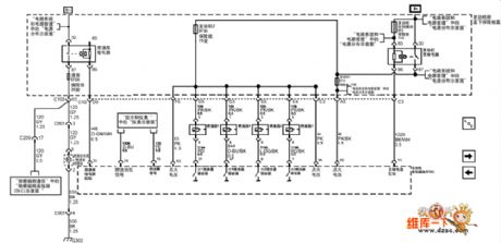
The Epica engine control system-fuel control-fuel pump control and injector circuit is as shown in the figure:
(View)
View full Circuit Diagram | Comments | Reading(620)
The simple separation amplifier circuit of photoelectric coupler
Published:2011/7/4 20:12:00 Author:Borg | Keyword: separation amplifier, photoelectric coupler

In the figure is the simple separation amplifier circuit of photoelectric coupler. This amplifier is used in the situation of low separation standard, the frequency width is 0~30kHz. In the circuit, RP1 is used to decide the bias, which makes the waveform distortion be the minimum. The DC bias and input signal are added together, which controls the forward current of the LED and makes A1 drive in with the constant current. The resistor R1 converts the current output by the photoelectric transistor into the voltage.
(View)
View full Circuit Diagram | Comments | Reading(586)
The typical application of LTC5507
Published:2011/7/6 3:11:00 Author:Christina | Keyword: typical application

The typical application of LTC5507 is as shown in the figure. C1 is the coupling capacitance of the RF input port, C2 is the peak keeping capacitance, both of C1 and C2 use the ceramic capacitor, the capacitive reactance is lower than 5Ω to reduce the ripple wave of C2. The capacities of C1 and C2 depend on the minimum input frequency fmin of the RF (the unit is MHz), the formula is C1=C21≥(30fmin). In this formula, the units of C1 and C2 are μF. Because the value of C2 will affect the conversion rate and the bandwidth, so C1=C2. The capacities of C1 and C2 can not be too large, or the frequency will exceed the minimum input RF frequency.
(View)
View full Circuit Diagram | Comments | Reading(1033)
The photoelectric coupler separation amplifier circuit of PWM modulation
Published:2011/7/4 20:22:00 Author:Borg | Keyword: photoelectric coupler, PWM modulation

After the impedance conversion by A1, the input signal of the circuit is past the integrator, time lag comparator A2 and PWM modulation circuit, then it is converted into a pulse signal which has some time width, its signal LEV is processed as the digit signals of 1 and 0. The pulse signal drive photoelectric coupler TLP512, which has some certain time width, can get the pulse signal of certain time width at the second stage, but the primary signal is separated. The phase reverser 4069 of the second stage receives this time width pulse signal. (View)
View full Circuit Diagram | Comments | Reading(935)
Epica engine control system subsystem circuit
Published:2011/7/6 3:13:00 Author:Christina | Keyword: Epica, engine control system, subsystem circuit
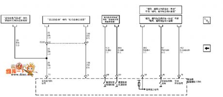
The Epica engine control system subsystem circuit is as shown in the figure:
(View)
View full Circuit Diagram | Comments | Reading(542)
Digital output angle sensor signal conditioner application circuit diagram
Published:2011/7/1 1:55:00 Author:Ecco | Keyword: Digital output , angle sensor , signal conditioner , application

the chart shows the UZZ9001 typical application circuit. C is the decoupling capacitor. SPI input / output interface is directly matched with a microcontroller (μC), which can be set by SCM UZZ9001. UZZ9001 angle measurement error is about ± 0.35o.
(View)
View full Circuit Diagram | Comments | Reading(776)
The application circuit diagram of 1B32 multiple pressure sensor
Published:2011/6/30 2:53:00 Author:Ecco | Keyword: application, multiple , pressure sensor

Excitation power can drive multiple bridge sensors after passing AD542, TIP32. AD542 is an op amp which uses Bi-FET as the input stage, and it play the role of starting buffer. TIP31 is the extension NPN power transistor with the maximum reverse voltage in 45V, the maximum collector current in 3A, maximum power consumption in 40W. The circuit can provide +10 V, 300mA excitation source in the temperature range of -25 ~ +80 ℃. When 333.3 GAIN of 1B32 is grounded, the gain is set to 333.3 times.
(View)
View full Circuit Diagram | Comments | Reading(931)
Transformer, RC circuit and direct-coupled amplifier circuit diagram
Published:2011/7/1 1:30:00 Author:Ecco | Keyword: Transformer, RC circuit , direct-coupled , amplifier

View full Circuit Diagram | Comments | Reading(867)
Using capacitor to reduce the cut-off frequency circuit diagram
Published:2011/6/30 22:51:00 Author:Ecco | Keyword: capacitor, reduce , cut-off frequency

The cut-off frequency of low-pass filter can be set under 1kHz by the external capacitors CSEL1, CSEL2 to meet the needs of narrow-band applications, and the circuit is shown as the chart.
(View)
View full Circuit Diagram | Comments | Reading(572)
Epica engine data sensor-ignition system circuit
Published:2011/7/6 20:43:00 Author:Christina | Keyword: Epica, engine, data sensor, ignition system
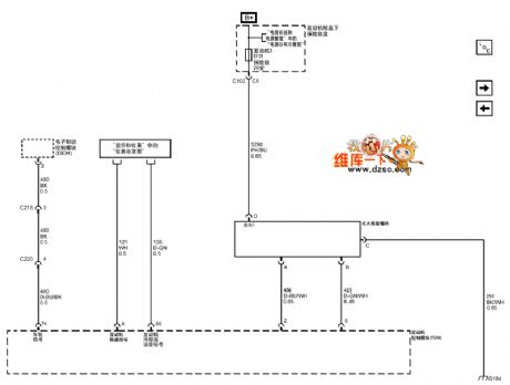
The Epica engine data sensor-ignition system circuit is as shown in the figure:
(View)
View full Circuit Diagram | Comments | Reading(501)
TL431 high-power adjustable circuit diagram
Published:2011/7/1 1:48:00 Author:Ecco | Keyword: high-power , adjustable


Precision voltage reference IC TL431 with T0-92 package is shown as the Figure 1. Its performance is continuously adjustable output voltage which is up to 36V, and the operating current range is 0.1. 100mA typical dynamic resistance is 0.22 Ω, and it has low output noise. Figure 2 is the typical application of the TL431, of which both ends of ③, ② feet output voltage V = 2.5 (R2 ten R3) V/R3. If you change the size of the resistance of R2, you can change the size of the output reference voltage. D5, D6, C2, C3 form the doubler circuit.
(View)
View full Circuit Diagram | Comments | Reading(4935)
Simple touch delay switch circuit diagram
Published:2011/6/27 4:41:00 Author:Ecco | Keyword: Simple , touch , delay switch

Many people live in high-rise housing have installed sound delay switch in front of their doors, they are easy to use, you can also save energy, but sometimes it did not convenient. This voice-activated switch is very sensitive that the slightest sound will cause it action, such as the sound of neighbors opening and closing door, firecrackers outside, and they will make your door lights be lit up, and it does not save power, but also affect the life of the lam. The circuit is very simple, when touching metal films, VT1 is turned on and charging for capacitor C2.
(View)
View full Circuit Diagram | Comments | Reading(1036)
Small (2-3 meters) neon electronic transformer circuit diagram
Published:2011/7/1 1:42:00 Author:Ecco | Keyword: 2-3 meters, neon , electronic transformer

View full Circuit Diagram | Comments | Reading(4180)
The typical application circuit of the LT5504
Published:2011/7/6 20:35:00 Author:Christina | Keyword: typical application

The typical application circuit of the LT5504 is as shown in the figure. The RF signal adds to the RF input port of LT5504 through the coupling capacitance (C1) and the 1:1 RF input transformer (T). R1 is the shunt resistor. The crystal frequency adds to the LO port through the C5. The Uo port gets the DC output voltage Vo through the voltage divider R2 and R5. JP is the jumper, because the R4>>R3, so when the JP is connection, the EN port connected with the high level to open the circuit, when the JP cuts off, the EN port connected with the low level to close the circuit, the chip is in the low power consumption mode.
(View)
View full Circuit Diagram | Comments | Reading(597)
Energy-saving fluorescent starter circuit diagram
Published:2011/6/28 2:49:00 Author:Ecco | Keyword: Energy-saving , fluorescent , starter

In the Figure, FU is fuse. C1, C2 are the bulk capacitors. C3, C4 are the starter capacitors. VD1, VD2, VD3, VD4 are the rectifier diodes. R1, R2 are the current limiting resistors. H is fluorescent tube or energy saving lamp. Before H turns on, the internal resistance is great, and the current is very low, and the power is added to the rectifier circuit composed of VD1 ~ VD4. C1, C2 choose the 1.5μ F capacitors with voltage in more than 400V. C3, C4 choose 0.01μF capacitors with voltage in more than 400V. VD1 ~ VD4 choose 1N4007 1A silicon rectifier diodes with voltage more than 400V. R1, R2 select 5W metal film resistors with more than 50 ~ 100Ω.
(View)
View full Circuit Diagram | Comments | Reading(2209)
A precise constant temperature controller circuit without temperature jumping area
Published:2011/7/4 20:46:00 Author:Borg | Keyword: temperature controller, temperature jumping area
The be knots of Q1 and Q2 are used as the temperature sensor. The 2.5V highly stable Vref is provided by the precise regulated integrated circuit U3(TL431) as the reference input of the window voltage comparators (U2C,U2D) and difference amplifier (U1C). The connection of U1A and U1B is for debugging and the balance of the input impedance of the amplifier. The voltage follower U1D works as the buffer separator, which sends the temperature differential voltage Vd, which is amplified by U1C, to the non-inverting terminal of the voltage comparator U2B.
(View)
View full Circuit Diagram | Comments | Reading(662)
| Pages:1604/2234 At 2016011602160316041605160616071608160916101611161216131614161516161617161816191620Under 20 |
Circuit Categories
power supply circuit
Amplifier Circuit
Basic Circuit
LED and Light Circuit
Sensor Circuit
Signal Processing
Electrical Equipment Circuit
Control Circuit
Remote Control Circuit
A/D-D/A Converter Circuit
Audio Circuit
Measuring and Test Circuit
Communication Circuit
Computer-Related Circuit
555 Circuit
Automotive Circuit
Repairing Circuit