Circuit Diagram
Index 1615
Three-Point Protection Circuit
Published:2011/7/5 5:58:00 Author:Robert | Keyword: Three-Point, Protection

The three-point protection circuit is shown in the picture. When there is a surge voltage flowing into the circuit, the gas discharge tube would guide the surge current to the underground. So that the equipments could get the protective effects.
The picture shows the three-point protection circuit. (View)
View full Circuit Diagram | Comments | Reading(705)
Three-Pole Gas Discharge Tube Shape Circuit
Published:2011/7/5 6:00:00 Author:Robert | Keyword: Three-Pole, Gas Discharge Tube, Shape

The picture shows the three-pole gas discharge tube shape circuit. (View)
View full Circuit Diagram | Comments | Reading(696)
AD651 F/V Conversion Circuit
Published:2011/7/5 6:05:00 Author:Robert | Keyword: F/V, Conversion

The F/V converter composed of AD651 is shown in the picture.
The picture shows the AD651 F/V conversion circuit. (View)
View full Circuit Diagram | Comments | Reading(783)
Two-Pole Gas Discharge Tube Shape Circuit
Published:2011/7/5 6:01:00 Author:Robert | Keyword: Two-Pole, Gas Discharge Tube, Shape

The picture shows the two-pole gas discharge tube shape circuit. (View)
View full Circuit Diagram | Comments | Reading(553)
Fluorescent lamp driver circuit composed of FET
Published:2011/7/4 23:42:00 Author:Lucas | Keyword: Fluorescent lamp , driver circuit , FET

Fluorescent tube is connected in the LC resonant circuit composed of L2 and C9. Bidirectional breakdown diode VD4 is starting circuit. When AC power is connected, VT2 gate potential increases by VD4; when the voltage exceeds the gate threshold voltage, VT2 is conducted. Thus, the resonant current folws C8, fluorescent wire, resonant capacitor C9, choke L2, the winding of drive transformer Tl by +25 V DC voltage, and the oscillation cycle is decided by C9, L2, and T1. Before the light iturning on, the resonant state is decided by the C9, L2, and VT1, VT2. (View)
View full Circuit Diagram | Comments | Reading(3361)
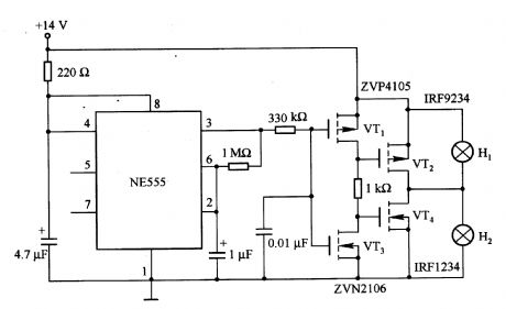
The lamp drive circuit using NE555
Published:2011/7/5 1:15:00 Author:Lucas | Keyword: lamp , drive circuit

In the circuit, the bulb Hl and H2 are connected in parallel. When Hl is lit; MOSFET tube VT4 is conducted, almost all the supply voltage is added at both ends of H1, then Hl is brightest. For lighting the bulb H2, t, it will generate 3Oms delay, then the end of bulb has been lit by filament light bulb, and the impact is that the impulse current is limited to be the steady-state current of lamp to extend lamp life. NE555is the oscillator circuit, andthe pin 3 outputs pulse signal.
(View)
View full Circuit Diagram | Comments | Reading(2581)
Biopotential / frequency converter composed of LM324
Published:2011/7/5 6:54:00 Author:Lucas | Keyword: Biopotential / frequency converter

The modulation circuit is composed of the high-gain differential amplifier, and it includes operational amplifiers Al and A2 and related discrete components. Regulating RPl can change the the gain of the electrode amplifier in the range of 100 times to 10,000 times, the biological potential is enlarged to a sufficient level to control the voltage frequency modulation circuit in the modulation circuit. The voltage frequency modulation circuit is composed of the reversible integrator A3 and two-level comparator A4. The integral slash increasing rate of A3 is 227xUl (V / μS), and the increasing positive and negative direction is decided by the VTl the boron dry state, which is controlled by the A4.
(View)
View full Circuit Diagram | Comments | Reading(10502)
A simple micro power transmitter field intensity indicator circuit diagram
Published:2011/6/30 3:32:00 Author:Ecco | Keyword: simple , micro power , transmitter , field intensity indicator

This circuit is a simple field intensity indicator, which is very sensitive for micro-power signal. Because the circuit is only used for the relative field strength, there is no standard, but you can make debugging easily! You can use the probe to measure modulator output end directly, the probe can measure incentive output.
(View)
View full Circuit Diagram | Comments | Reading(1337)
Touching delay lamp switch circuit(8)
Published:2011/6/30 5:12:00 Author:Ecco | Keyword: Touching , delay lamp , switch

The chart shows the touching delay light switch with good performance , the circuit is characterized by: minimal static power consumption; switch has only two terminals outside, which can replace the ordinary switch. Circuit delay time is mainly decided by C1, R2 discharging time constant. In addition, the trigger sensitivity of VT1 and the magnification of VT2 have a significant impact on the delay time.
(View)
View full Circuit Diagram | Comments | Reading(596)
Robot control circuit composed of transistor and NE555
Published:2011/7/1 21:12:00 Author:Lucas | Keyword: Robot control , transistor


Figure 2-33 (a) is the action schematic diagram of the robot closing to the object. When there is no objects in front of the robot, it will go forward in the straight line; when there is an object in left or right side of the robot,it will turn left or right to close to the object. Figure 2-33 (b) is the block diagram to achieve this action. Figure 2-33 (c) is the actual circuit, in the circuit, NE555 is the multivibrator to produce pulse signal to modulate the infrared light emitted by infrared light-emitting diode TLNlO5, and the purpose is to avoid interference from other light. NE555 oscillation frequency is l0 kHz.
(View)
View full Circuit Diagram | Comments | Reading(2889)
Touching delay lamp switch circuit(7)
Published:2011/6/30 5:21:00 Author:Ecco | Keyword: Touching , delay lamp , switch

The circuit shown in the chart is the delay lamp which uses the principle of self-oscillation to improve trigger sensitivity. The circuit is composed of the self-excited multivibrator, touch switch, power supply circuit and thyristor switch. The circuit delay time is mainly determined by C1, R4 discharging time constant, and at the same time the R3's resistance, VT1 magnification and touching time also have an impact on the delay time.
(View)
View full Circuit Diagram | Comments | Reading(1451)
Motor time division control circuit composed of transistor and NE555
Published:2011/6/30 21:06:00 Author:Lucas | Keyword: Motor , time division, control circuit , transistor


Figure 2-32 (a) shows the time control diagram, and the motor is operated by the switch S1. When Sl is turned to 1, the power driver circuit provides current to the motor for running; When S1 is turned to 2, the drive current is cut off, and the electric motor is used as a generator to hold out the back electromotive force by the sampling circuit. S1is turned to 2 by the sampling circuit, the back electromotive force is used as a sample to keep until the next on / off cycle of S1. Keeping the hold voltage and speed settings voltage be same can provide power for the motor control circuit.
(View)
View full Circuit Diagram | Comments | Reading(2550)
Touching delay lamp switch circuit(6)
Published:2011/6/30 5:17:00 Author:Ecco | Keyword: Touching, delay lamp, switch

In the circuit shown as the chart, the delay time is mainly decided by R5, C discharging time constant, VT1 magnification and the length of touching time. Typically, a manual touching on M, light E can be lit for 1 ~ 2min.
(View)
View full Circuit Diagram | Comments | Reading(536)
Touching delay lamp switch circuit(5)
Published:2011/7/1 2:34:00 Author:Ecco | Keyword: Touching , delay lamp , switch

The chart shows the touching delay lamp switch circuit with only two outside Lead which can directly replace an ordinary switch to be connected to lighting circuits. The circuit delay time is mainly decided by C1, R3 charging time constant, their value can be adjusted to change the lights lighting duration time.
(View)
View full Circuit Diagram | Comments | Reading(897)
Diode dimmer switch circuit
Published:2011/6/30 2:31:00 Author:Ecco | Keyword: Diode , dimmer, switch circuit

In the circuit shown as the chart, when the S1, S2 are closed, light E has normal light; S1 remains closing, S2 is open, E emits dark light; if S1 is open, the light E is off whether S2 is open or not.
(View)
View full Circuit Diagram | Comments | Reading(1091)
Electronic energy saving lamp (1)
Published:2011/6/30 2:27:00 Author:Ecco | Keyword: Electronic, energy saving , lamp

VT1, VT2 choice MTE13003 ~ 13005 high-power tube, and β value is between 20 to 40. T1, T2 need to be made by yourself: the three coils of T1 are available in different colors with Φ0.4mm single strand of copper wire wound on igh frequency magnetic ring with internal diameter in Φ10mm, and L1, L2 around 6.5 turns in parallel, L3 has 2 turns. T2 uses EI ferrite core with cross-sectional area in 10mm × 7mm, then L4 and L5 use Φ0.27mm high-intensity polyester enameled wire wound. L6 uses Φ0.8mm high-strength polyester with around 13 turns. E uses 35W, 12V low-voltage halogen bulb.
(View)
View full Circuit Diagram | Comments | Reading(3038)
Time Relay (the 3rd)
Published:2011/7/5 2:27:00 Author:Felicity | Keyword: Time Relay (the 3rd)

Work of the circuit
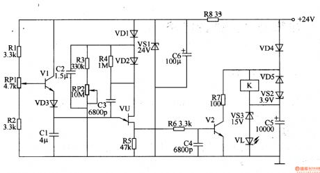
The circuit consists of regulator filter circuit, the delay charge and discharge circuit and relay control circuits. (It is showed in the picture 8-137.)
Regulator filter circuit consists of Resistor R8, zener diode VS1 and filter capacitor C6.
The delay charge and discharge circuit consists of Resistors Rl-R5, capacitor RPl and RP2, transistor Vl, capacitors Cl-C3, diodes VDl-VD3 and single-junction transistor VU.
Relay control circuits consists of resistors R6 and R7, capacitors C4 and C5, diode VD4 and VD5, voltage regulator diode VS2 and VS3, the transistor V2, LED VL and relays K. (View)
View full Circuit Diagram | Comments | Reading(596)
Time Relay (the 2nd)
Published:2011/7/5 2:28:00 Author:Felicity | Keyword: Time Relay (the 2nd)

Work of the circuit
The circuit consists of +12V power circuit, monostable circuit and relay control circuits. (It is showed in the picture 8-136.)
Power circuit consists of power transformer T, rectifier diode VDl, VD2, three-terminal voltage regulator integrated circuit ICl and filter capacitor Cl, C2.
Monostable circuit consists of potentiometer RP, diodes VD3, capacitors C3, C4, time-base integrated circuit IC2 and the normally closed contact relay Kl.
Relay control circuits consists of resistors Rl, R2, relay Kl, K2, diodes VD4 and LED VL. (View)
View full Circuit Diagram | Comments | Reading(585)
Batch-type cockroach killer circuit
Published:2011/7/5 21:28:00 Author:Christina | Keyword: Batch-type, cockroach, killer circuit

The batch-type cockroach killer circuit is as shown in the figure. It uses the DC voltage to kill the cockroaches. But because the cockroaches are very sensitive to the electric field, they can not climb the high-voltage power net, so this circuit is the batch-type.
(View)
View full Circuit Diagram | Comments | Reading(2059)
Monolithic liquid crystal display range finder circuit composed of the intelligent ultrasonic ranging integrated circuit 4Y4
Published:2011/7/5 21:22:00 Author:Christina | Keyword: Monolithic, liquid crystal display, range finder, intelligent, ultrasonic, ranging integrated circuit

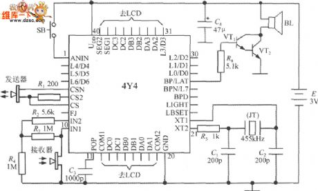
The monolithic liquid crystal display range finder circuit which is composed of the intelligent ultrasonic ranging integrated circuit 4Y4 is as shown in the figure. The meter is composed of the ultrasonic transmitter, the receiver, the LCD displayer, the button switch and the buzzer (or the speaker), in order to simplify the lead, we directly weld the 4Y4 at the back of the LCD display board. The pin-2 ~ pin-4, pin-8, pin-23 ~ pin-26 and pin-28 ~ pin-30 are not needed. R1 is the current-limiting resistance of the transmission circuit. R2~R4 are the external components of the receiving amplifier.
C3 is the automatic reset capacitance. The crystal oscillator circuit uses the low-cost 455kHz piezoelectric ceramic to instead of the quartz crystal (JT), C1 and C2 are the oscillation capacitance. SB is the button switch.
(View)
View full Circuit Diagram | Comments | Reading(1474)
| Pages:1615/2234 At 2016011602160316041605160616071608160916101611161216131614161516161617161816191620Under 20 |
Circuit Categories
power supply circuit
Amplifier Circuit
Basic Circuit
LED and Light Circuit
Sensor Circuit
Signal Processing
Electrical Equipment Circuit
Control Circuit
Remote Control Circuit
A/D-D/A Converter Circuit
Audio Circuit
Measuring and Test Circuit
Communication Circuit
Computer-Related Circuit
555 Circuit
Automotive Circuit
Repairing Circuit