
Circuit Diagram
Index 55
220V Power Line Interface
Published:2013/10/28 20:18:00 Author:lynne | Keyword: Power Line Interface

This simple 220V power interface is intended as an interface for monitoring electric equipments and devices using a computer. The interface only senses whether the device being monitored is turned on or off. The most important aspect of the circuit is the galvanic isolation between the AC main line being monitored and the interface to the computer. This is done with the use of the optocoupler IC TIL111 but a suitable replacement can be used too.
Main power live interface circuit diagram
To avoid having to modify the circuit for each device being monitored, the circuit monitors the device’s AC power line directly. The resistor R1 lets a current of around 0.5 mA through the optocoupler LED. The other half of the current is rectified through the diode D1. It is obvious that the current to the optocoupler LED is half wave rectified. This means that the phototransistor part of the optocoupler receives only light impulses of around 100uA. The capacitor C1 filters out the current pulsation and maintains a smooth output current. In case the current pulsation is needed, just remove C1. (View)
View full Circuit Diagram | Comments | Reading(1658)
STEPPER MOTOR CONTROLLER Circuit
Published:2013/10/27 21:14:00 Author:lynne | Keyword: STEPPER MOTOR CONTROLLER

The direction of rotation is determined by the FORWARD and REVERSE switches and the motor does not take any current when a switch is not pressed. (View)
View full Circuit Diagram | Comments | Reading(2191)
REACTION TIMER GAME Circuit
Published:2013/10/27 21:10:00 Author:lynne | Keyword: REACTION TIMER

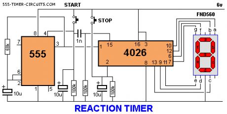
This is a game for two players. Player 1 presses the START button. This resets the 4026 counter chip and starts the 555 oscillator. The 555 produces 10 pulses per second and these are counted by the 4026 chip and displayed on the 7-Segment display. The second player is required to press the STOP button. This freezes the display by activating the Clock Inhibit line of the 4026 (pin 2).Two time-delay circuits are included. The first activates the 555 by charging a 10u electrolytic and at the same time delivering a (high) pulse to the 4026 chip to reset it. The second timer freezes the count on the display (by raising the voltage on pin 2) so it can be read.
(View)
View full Circuit Diagram | Comments | Reading(1595)
ROULETTE Circuit
Published:2013/10/27 21:09:00 Author:lynne | Keyword: ROULETTE Circuit
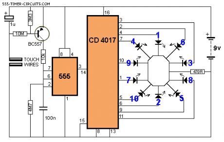
This circuit creates a rotating LED that starts very fast when a finger touches the TOUCH WIRES. When the finger is removed, the rotation slows down and finally stops. (View)
View full Circuit Diagram | Comments | Reading(1319)
3A Adjustable Power Supply
Published:2013/10/24 20:14:00 Author:lynne | Keyword: Adjustable Power Supply

This is a compact adjustable power supply that delivers a stable voltage and currents up to 3 amperes. The circuit is very conventional and its voltage output can be varied from 1.25 volts to 25 volts.The main module is the LM350 IC which integrates a voltage regulator and a power stage. It also has a built-in overload protection which activates at 30 watts of power dissipation. The voltage output is set by connecting the “adj” pin of the IC to the voltage divider made of R1 and P1.
The output voltage can be calculated using the following formula:
1.25V x (1 + P1/R1)
where the P1 value is between 0 and 2.5 KΩ. Capacitor C1 is a common ripple filter while capacitors C2 and C3 improves the regulation. The diodes D1 and D2 serves as protection for the regulator IC when the IC output is turned off. Resistor R1 is 120Ω. This ensures that the minimal load current for the IC (around 3.4mA) is high enough to maintain good performance.
3 Ampere power supply circuit schematic
One thing that is most important in building the electronic circuit: provide adequate heatsink for the LM350 IC. The power dissipation at the IC is very high, around 85 watts.Consider that the heat resistance of a TO-3 package is 1.5oC/W and the maximum allowable temperature is 150oC. If a heatsink is used with a heat resistance of 1.5oC/W, when the total heat resistance is 4oC/W. At 30 watts dissipation and 25oC outside temperature, the resulting internal IC temperature is 145oC. Once this dissipation level is reached, the internal protection activates shutting down the IC.
One way to avoid high dissipation levels is to use a lower voltage transformers when needed output voltages are low. To put it simply: if you are using the circuit to supply voltages around 9 volts, do not use a 25 volts transformer but use a lower voltage one instead (e.g. 12 or 15 volts). (View)
View full Circuit Diagram | Comments | Reading(1474)
Honeywell SC8105-001 IR Photodarlington Transistor
Published:2013/10/24 20:12:00 Author:lynne | Keyword: Photodarlington Transistor

Honeywell SC8105-001 Features & Specs
Low cost
Popular T-1 plastic package
Opaque black visible light filter to exclude visible light
High sensitivity
Acceptance angle: ±10o
Wavelength: 935nm peak (Infrared spectrum)
Light current: 500µA Min
Dark current: 0.25µA Max
(View)
View full Circuit Diagram | Comments | Reading(1163)
Light Activated Siren Circuit
Published:2013/10/24 20:10:00 Author:lynne | Keyword: Light Activated Siren Circuit
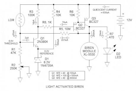
This light activated siren could make an unknowing “victim” wet his pants when turning on the lights in a dark room. This thing is LOUD! Power into the module is 3W and produces a 123db sound level from its 50mm diameter diaphragm. It wavers between 2kHZ and 4kHZ. An LDR senses ambient light level and switches on the power to the siren module via a transistor comparator and a darlington driver.The threshold is adjustable.
Schematic of the light activated siren
Input divider
The LDR and R1 & R2 form a voltage divider whose output voltage is light dependent. As the light level increases, the junction of the LDR and R1 increases. When it reaches 6.8V, Q1 turns on and subsequently triggers the alarm. Pot R2 calibrates the divider for the required light level threshold. The voltage out of the divider may be measured with a voltmeter so you can see what is happening as you debug the circuit.
Transistor comparator
Q1 is an NPN transistor applied as a comparator. Never heard of a transistor comparator before—well now you have—not exactly high performance with limited gain and 600mV offset, but fully functional and perfect for this application. Q1 has a minimum current gain (hFE) of 40 at low current levels. When the LDR is fully off, the Vbe of Q1 is -6.2V. Most transistors are rated for 6 to 7V reverse bias on the base to emitter junction.
Voltage reference
D1 is a 6.2V zener diode that is used as a voltage reference. R4 provides the required bias current. The cathode of the zener is a low impedance node for the emitter of Q1 to work into.
Darlington driver
Q2 & 3 are discrete high current TO-92 PNP transistors wired in the darlington configuration. In this configuration, the hFE is essentially squared so that it provides adequate current gain to easily drive the 280mA load.
Positive feedback
R5 provides about 1% positive feedback to insure positive switching as soon as the threshold is exceeded. This is also called hysteresis. R5 may be adjusted for best performance.
Circuit not tested
Generally the circuits I submit to electroschematics.com have been built and tested. This one has not, but I have a high level of confidence that it will work OK. It simulates fine in my cranial simulator.
Circuit operation
When light falls on the LDR, its resistance decreases and the voltage at the junction of the LDR and R1 increases. When the voltage exceeds 6.8V, Q1 turns on. The collector current of Q1 is the base current of the darlington driver and turns it on. This is called a high-side driver because it works against the positive bus. When voltage appears across the siren module, the voltage across and current through R5 reverses polarity and forces the voltage at the input voltage divider slightly higher thus causing it to “snap” on positively. When three transistors are wired like this, the DC gain is so high that a minute amount of leakage can cause circuit malfunction. R3 and R6 provide paths for leakage current thus insuring reliable operation.
For the future
Temperature activated siren circuit—actually you can do this now by simply replacing the LDR with an NTC thremistor.
Undocumented words and idioms (for our ESL friends)
debug—troubleshooting term. Literally, to get the insects out. From the early days of relay based computers where a moth took down a system when its wings got into the contacts of a relay. (View)
View full Circuit Diagram | Comments | Reading(1135)
General Purpose Power Supply
Published:2013/10/23 20:30:00 Author:lynne | Keyword: General Purpose Power Supply
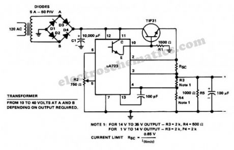
This general purpose power supply can e used for supply output voltages from 1 to 35V. The line transformer should be selected to give about 1.4 times the desired output voltage from the positive side of filter capacitor C1 to ground. Potentiometer R2 sets the output voltage to the desired value by adjusting the reference input.Rsc is the current limit set resistor. Its value is calculated as:
Rsc = 0.65V/IL
For example, if the maximum current output is to be 1A, Rsc = 0.65/1 = 0.65ΩThe 1kΩ resistor, Rs, is a light-loaded resistor designed to improve the no-load stability of the supply.
General power supply circuit schematic
(View)
View full Circuit Diagram | Comments | Reading(0)
Universal Power Supply Circuit
Published:2013/10/23 20:29:00 Author:lynne | Keyword: Universal Power Supply Circuit

This universal power supply contains, beside the bridge rectifier, a voltage stabilizer (78xx) and a pnp power transistor. This combination allow a load current up to 5 A. As you know a voltage stabilizer in a TO-220 package can deliver up to 1A. The additional power transistor takes the load current of about 200mA.The transformer voltage must be greater with 4V than DC stabilized voltage. C1 is calculated for 1A/1000uF, so at 5A C1 must have 4700uF. Both, transistor and voltage stabilizer must be mounted on a heatsink.
Universal power supply circuit diagram
(View)
View full Circuit Diagram | Comments | Reading(1523)
GFI Ground Fault Interrupter Wall Wart
Published:2013/10/23 20:28:00 Author:lynne | Keyword: GFI Ground Fault Interrupter Wall Wart
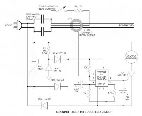
I always wondered what was inside one of these clever devices, so I found one in my junk box and popped the lid—it was from a defunct blow hair dryer—never throw one of these away because the GFI unit long outlives the hair dryer and has many experimental uses. To get it apart, I had to make a special screw driver bit to remove the tamper resistant screws.
Inside was something that resembles a relay, a circuit board and a tiny current transformer. This did not happen by itself—that is why I cannot accept the theory of evolution—there was a designer!
The contacts resemble those of a relay, but are actuated manually via a button that protrudes through the cover, and released via a small solenoid operated plunger. There is a test pushbutton that operates a crude leaf contact on the small circuit board.
I traced out the circuit carefully and drew up the schematic. The IC is probably a variant of the Fairchild RV4141A or RV4145A because the pin out does not exactly agree with either device. Regardless, there are numerous ways of applying IC’s and the schematic in the application note is merely a guide. The current transformer is very likely a 1:1000 turns ratio device.
Ground Fault Interrupter Schematic
How it works
You will notice that the parallel power leads make a single turn through the primary of the current transformer (CT). The flux field of the source lead is cancelled by the flux field in the return lead so the net result is zero and the CT sees no primary current. Should these currents ever become unequal (as in a ground fault condition), the CT senses this difference and induces current into the 1000 turn secondary. The secondary current is low, but the load resistance is 1M, so it develops significant voltage. This voltage is sufficient to exceed the comparator threshold voltage of the IC and fire the SCR. When the SCR fires, it energizes the solenoid coil and jerks an iron slug toward the center of the coil. Attached to this iron slug is a stainless steel pin that actuates the mechanical release for the electrical contacts. When the contacts are open, the ground fault current is interrupted and the appliance is off-line. It remains off until the mechanical reset button is pressed.
Note that this is for an unbalanced fault condition in which the current flows to ground. It cannot provide protection for a balanced fault such as holding both ends of a suicide cord in either hand.
C1 prevents any DC bias current from flowing through the CT secondary. It does not take much primary current to saturate the core and degrade its performance. RV1 is a MOV transient suppressor—this is required to pass the 5000V UL/CSA/VDE transient voltage test.
There is also a small red wire that also goes through the CT opening—this is the test turn and it connects to a 15K resistor. When the test pushbutton is pressed, it connects the 15K resistor across the line and forces a low unbalanced current (7mA) through the primary. This low current simulates a limited ground fault condition that is similar to a mild electrical shock. Actual sensitivity is 4.8mA—I measured it by substituting various resistors. UL/CSA/VDE standards assume that anything below 5mA is non-life threatening.
Preventing nuisance trips is a requirement. This is what the 6.8uf gate to cathode capacitor is all about—it swamps out noise pulses, but charges up to the SCR gate voltage threshold when there is a real ground fault signal present.
Components to save for future experimentation
Current Transformer
Solenoid
SCR (View)
View full Circuit Diagram | Comments | Reading(1711)
OverVoltage Protection Circuit
Published:2013/10/22 21:52:00 Author:lynne | Keyword: OverVoltage Protection Circuit
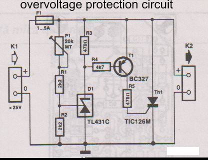
This overvoltage protection or crowbar protection circuit is used where we need protection against high voltage surge. The circuit has a few components, it is very easy to build and will protect your electric equipment againg overvoltages. The crowbar circuit must be mounted between power supply and the protected device.
The over voltage protection circuit is based on brute force: when the power supply voltage increases too much a thyristor shortcircuit the output. This mean that the overvoltage is quickly removed from equipment power terminals and F1 fuse will burn.
The voltage at which the crowbar protection starts is set between 5V and 25V with P1:
adjust P1 at maximum resistance value.
temporarily replace the fuse with a wire and connect the crowbar circuit at a variable power supply.
adjust the current limitation at 1 A si the output voltage at the desired value to activate crowbar protection.
slowly rotate P1 until activation of the thyristor (when the current limitator engages)
The overvoltage (crowbar) circuit is now set. Replace the wire bridge with a fuse (5A). In repaos state the circuit take 1 mA.
Over Voltage/Crowbar Protection Circuit Diagram
(View)
View full Circuit Diagram | Comments | Reading(2903)
Reverse Polarity Protection Battery Charger
Published:2013/10/22 21:50:00 Author:lynne | Keyword: Reverse Polarity Protection Battery Charger

This reverse polarity protection NiCd battery charger can charge up to 7 NiCd batteries connected in series. This number can be increased if the power supply is increased with 1.65V for each supplementary battery. If T2 is mounted on a proper heatsink, the input voltage can be increased at a maximum of 25V.
Unlike most of comercial NiCd chargers available on the market, this charger has a reverse polarity protection. Another great quality is that it does not discharge the battery if the charger is disconnected from the power supply.
Usually , NiCd batteries must be charged in 14 hours at a charging current equal with a tenth percent from battery capacity. For example, a 500 mAh is charged at 50 mA for 14 hours. If the charging current is too high this will damage the battery.
The level of charging current is controlled with P1 between 0 mA – 1000 mA. T1 is opened when the NiCd battery is connected with the right polarity or if the output terminals are empty. T2 must be mounted on a heatsink.
If you cannot obtain a BD679, then replace it with any NPN medium power Darlington having the output parameters at 30V and 2A. By lowering R3 value the maximum output current can be increased up to 1A.
NiCd Battery Charger Circuit Diagram
(View)
View full Circuit Diagram | Comments | Reading(1622)
Desktop PC Linear Power Supply Circuit
Published:2013/10/22 21:48:00 Author:lynne | Keyword: Desktop PC Linear Power Supply Circuit
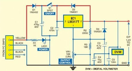
Useful for electronics hobbyists, this linear workbench desktop power supply circuit converts a high input voltage (12V) from the SMPS of a PC into low output voltage (1.25 to 9 volts). An adjustable three-pin voltage regulator chip LM317T (IC1) is used here to provide the required voltages. The LM317T regulator, in TO-220 pack, can handle current of up to 1 amp in practice.
Desktop PC power supply circuit diagram
The diagram shows the circuit of the desktop power supply. Regulator IC LM317T is arranged in its standard application. Diode D1 guards against polarity reversal and capacitor C1 is an additional buffer. The green LED (LED1) indicates the status of the power input. Diode D2 prevents the output voltage from rising above the input voltage when a capacitive or inductive load is connected at the output. Similarly, capacitor C3 suppresses any residual ripple.
Connect a standard digital voltmeter in parallel with the output leads to accurately set the desired voltage with the help of variable resistor VR1. You can also use your digital multimeter if the digital voltmeter is not available. Switch on S1 and set the required voltage through preset VR1 and read it on the digital voltmeter.Now the power supply is ready for use.
The circuit can be wired on a common PCB. After fabrication, enclose the circuit in a metallic cover. Then open the cabinet of your PC and connect the input line of the gadget to a free (hanging) four-pin drive power connector of the SMPS carefully. (View)
View full Circuit Diagram | Comments | Reading(1126)
Variable Power Supply with 78XX regulator
Published:2013/10/21 20:41:00 Author:lynne | Keyword: Variable Power Supply
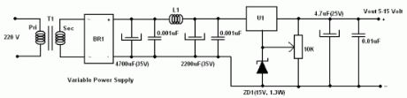
This variable power supply is using 7805, 7809, 7812 or 7815 voltage regulators, where the last 2 digits represents the maximum output voltage of the IC.This circuit offers excellent ripple rejection, eliminates mains hum, and has a design using a pi filtered C-L-C.
A core should be chosen to work within the specific frequency as stated by the manufacturer. L1 is a powder core and has 32 turns of 0.75mm wire.
Variable Power Supply Circuit Diagram
The transformer has a 240V primary and has a secondary rated 24V at 2A. The bridge rectifier contains 4 diodes, their current rating needs to be high with respect to the transformers output current; if not the current may damage the diodes. C1 is the mainfiltering capacitor, the supply is further smoothed by the combination of L1 and C3. C2 and C4 are decoupling capacitors; their action further reduce ripple factor.
The regulator 78xxr, U1 utilizes the action of zener diode ZD1 which is in parallel with the potentiometer, R1. The tuning action of R1 produces a variable regulator output. The output voltage is variable from the regulator output to the regulator output plus the zener voltage. E.G. A 7805 regulator and 10V zener give an output adjustable from 5 to 15 Volts. The regulator may be changed to provide different output voltages as may the zener. the zener should be rated a minimum of 1.3 Watts.
T1 Transformer 10:1 Secondary 24V @ 2ABR1 Bridge Rectifier 50V PIV 2A ratingU1 7805 N.B. This may be changed for different output voltages e.g. 7812 for higher output voltageZD1 15V zener @ 1.3W (View)
View full Circuit Diagram | Comments | Reading(2349)
555 (TLC555) Relay Driver Circuit
Published:2013/10/21 20:33:00 Author:lynne | Keyword: Relay Driver Circuit
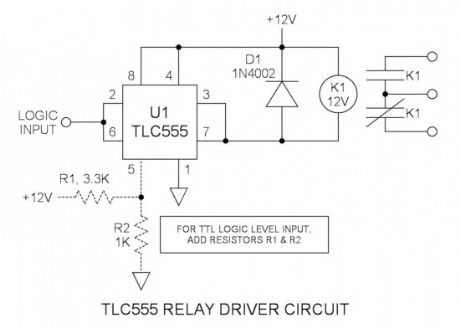
Many integrated circuits have undocumented features or abilities. This is one of them. The TLC555 output (pin 3) can sink a 100mA load to 1.28V. The open drain transistor reset (pin 7) can sink 100mA to 1V. Tying both lines together is permissible because they are logically the same polarity and this potentially doubles the sink current ability to 200mA. This is ideal for driving my 133mA relay coil.The input also has the undocumented, but better known, feature of a Schmitt trigger that provides positive switching.
555 Relay Driver Schematic
Output current rating (pin 3): TLC555 vs. NE555
(Vcc = 15V)
TLC555
NE555
Source current
10mA
200mA
Source mode saturation voltage
Vcc-0.8V
Vcc-2.5V
Sink current
100mA
200mA
Sink mode saturation voltage
1.28V
2.5V
While it can be seen that the NE555 has the higher current rating, its saturation voltage is grossly inferior and this is a detriment in driving loads without excessive voltage drop. Also it can be seen that the TLC555 is much like TTL in that its sourcing ability is far less than its sinking ability. However for driving a relay, we are interested only in current sinking properties. (View)
View full Circuit Diagram | Comments | Reading(1720)
Variable Power Supply with UA78G/UA79G
Published:2013/10/21 20:31:00 Author:lynne | Keyword: Variable Power Supply
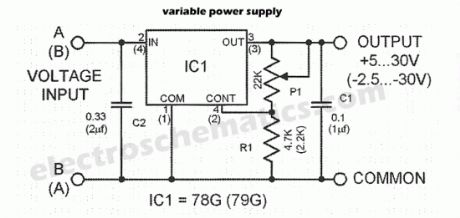
A stable variable power supply with an adjustable output voltage from 5 volts to 30 volts can be easily constructed with the regulator ICs UA78G or UA79G. These ICs differ from the common three-terminal regulator since their output voltages are adjustable by a voltage level at their control inputs. The maximum current delivered by these ICs is 1 ampere.
The unregulated voltage must be at least 5 volts higher than the desired output level to maintain stability. The input voltage however must not exceed 40 volts. The maximum dissipation of the IC is 15 watts.
The variable power supply circuit presented here is designed to give maximum voltage level of 28 volts. If P1 is replaced with 25K potentiometer, the regulator can deliver up to a maximum of 30 volts. Capacitors C1 and C2 stabilize the IC and they must be connected as close as possible to the IC terminals.
UA78G/UA79G power supply circuit diagram
(View)
View full Circuit Diagram | Comments | Reading(1817)
Single Transistor Amplifier Revisited – Part 2
Published:2013/10/20 20:23:00 Author:lynne | Keyword: Single Transistor , Amplifier
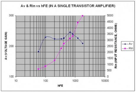

The goal of this series is to maximize the voltage gain of the single transistor amplifier. I had always thought that hFE had a profound effect upon voltage gain, so I set out to determine how much—the results surprised me. Then I went through another exercise to determine input resistance (Rin)—this is a grey area to most.
Graph of Voltage Gain & Input Resistance as a function of hFE
Transistor Selection
A number of transistors were added to those used in Part 1. This included a MPS6515 and a suspected “hot device” MPSA18 that turned out to be not as hot as I had predicted. Also, I added a 2N5088 and two very high hFE D3854 sample transistors that I had obtained from General Electric over 30years ago…no specs for this device can be found on the web, but I had had the foresight to write the hFE on the bag (hFE = 1500 to 3000).
Preface to the update
The initial data was in error due to a near resonant effect in the amplifier—this resonance caused unusually high voltage gain. After correcting the problem, I retook the data and updated the report.
Av is surprisingly stable
I would have thought with so wide a selection of transistors (nine in all), with a great range of manufacturers, packages, manufacturing dates, voltage ratings, current ratings, etc. that the curve would be lumpy with at least one or two anomalies that could not connect properly. However, such was not the case because it is apparent that voltage gain is largely independent of hFE. Note that the external circuit parameters likely have a significant effect, so any duplication of this exercise must be made under the same conditions.
Why the quest for high Av? Everyone wants “hot” amplifiers—gutless amplifiers are depressing. Perhaps you do not need all this voltage gain—in that case, it can be used to reduce distortion and noise via negative feedback—I am not suggesting that this open loop amplifier has low distortion—we will discuss that in future parts. Also, the conclusion of this series will introduce an amplifier with incredible gain performance.
Effective Av with a 2.2K resistor @ 3.2mA is approx 225—keep this number in mind.
Schematic of test setup
(View)
View full Circuit Diagram | Comments | Reading(1441)
USB DC Power Supply from Cigar Lighter Socket
Published:2013/10/20 20:14:00 Author:lynne | Keyword: USB DC Power Supply from Cigar Lighter Socket
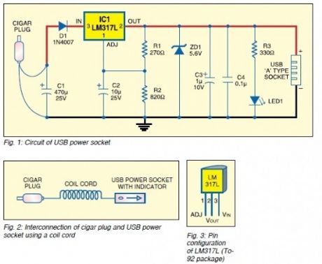
The diagram shows the circuit of a versatile USB power socket that safely converts the 12V battery voltage into stable 5V. This circuit makes it possible to power/recharge any USB power-operated device, using in-dash board cigar lighter socket of your car.
The DC supply available from the cigar lighter socket is fed to an adjustable, three-pin regulator LM317L (IC1). Capacitor C1 buffers any disorder in the input supply. Resistors R1 and R2 regulate the output of IC1 to steady 5V, which is available at the ‘A’ type female USB socket. Red LED1 indicates the output status and zener diode ZD1 acts as a protector against high voltage.
USB Power Socket Circuit Diagram
Assemble the circuit on a general-purpose PCB and enclose in a slim plastic cabinet along with the indicator and USB socket. While wiring the USB outlet, ensure correct polarity of the supply. For interconnection between the cigar plug pin and the device, use a long coil cord as shown in Fig. 2. Pin configuration of LM317L is shown in Fig. 3. (View)
View full Circuit Diagram | Comments | Reading(1193)
Cheap DC Voltage Doubler Circuit
Published:2013/10/20 20:12:00 Author:lynne | Keyword: Cheap DC Voltage Doubler Circuit

This is a cheap DC Voltage Doubler Circuit diagram, which requires a few components and will deliver 10V from a 5V power supply. If the oscillator must be built from a non-functional gate then is required 2 more components: R1 and C3.The most important parameters of this voltage doubler circuit are given in the table below. Note that because of the IC tolerances these data may have some differences.
Voltage doubler circuit diagram
(View)
View full Circuit Diagram | Comments | Reading(1156)
Inverted 555 Timer Circuit
Published:2013/10/17 20:26:00 Author:lynne | Keyword: Inverted 555 Timer Circuit
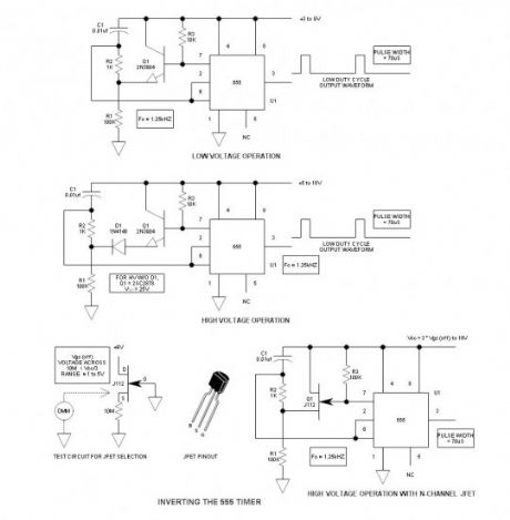
Whenever I use the 555 timer, it seems that the output polarity is invariably incorrect, and the way the 555 functions, it normally cannot generate a duty cycle of less than 50% — 90% yes, 10% NO! This inverted 555 circuit generates duty cycles of less than 50%. Everything works the same except for the polarity. Why not simply invert the output with a transistor? Will not that do the same? Legitimate question… Actually NO, because a transistor that inverts the output cannot provide the desirable totem pole source/sink output function of pin 3. And there is another reason that we will get in the future—this is a 555VCO circuit that requires the inverted timer.
Inverted 555 Timer Schematic
The schematic shows (3) circuits, because one circuit does not work well over the entire Vcc range.
The first simply uses a “normal” 2N3904 garden variety transistor, and this works well when Vcc < 9V. When Vcc > 9V, the base to emitter junction starts to zener and disrupts operation. Transistor base to emitter junction zeners a little above -6V.
The second circuit adds D1 to the emitter of Q1 in order to increase VEBO. With this mod, Vcc may be increased to the 18V limit. However, D1 may be eliminated if we use the special 2SC2878 switching transistor that has a VBEO rating of -25V. These devices are no longer in production, but are available on eBay—every serious experimenter should have a few in his component collection. The types now in production use the tiny SO-23 SMD package.
The third circuit uses a J112 N-Channel JFET for Q1. The JFET is a curious device that works well for the application provided we allow for the VGS(OFF) parameter. VGS must be less than Vcc /3. (e.g. if Vcc = 9V, VGS(OFF) must be less than 9V /3 or 3V for proper operation). Since the VGS(OFF) parameter is sloppy (-1 to -5V), the device must be selected—to the left is a simple test circuit—actually, most devices will work OK. The J112 should also be in every serious experimenter’s component collection. (View)
View full Circuit Diagram | Comments | Reading(1405)
| Pages:55/2234 At 204142434445464748495051525354555657585960Under 20 |
Circuit Categories
power supply circuit
Amplifier Circuit
Basic Circuit
LED and Light Circuit
Sensor Circuit
Signal Processing
Electrical Equipment Circuit
Control Circuit
Remote Control Circuit
A/D-D/A Converter Circuit
Audio Circuit
Measuring and Test Circuit
Communication Circuit
Computer-Related Circuit
555 Circuit
Automotive Circuit
Repairing Circuit