
Circuit Diagram
Index 54
12V LDO Solar Charge Controller
Published:2013/11/5 19:11:00 Author:lynne | Keyword: LDO Solar Charge Controller
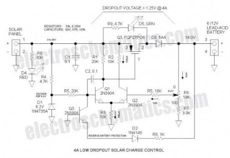
This Low Dropout Voltage (LDO) solar charge controller uses a simple differential amplifier and series P channel MOSFET linear regulator—their compatibility seems like a marriage made in heaven. Voltage output is adjustable. It is mainly intended for charging 12V lead-acid batteries.
Solar Charge Controller Specifications
Solar panel rating: 50W (4A, 12V nominal) (open circuit voltage: 18 to 20V)
Output voltage range: 7 to 14V (adjustable) (not recommended for 6V applications)
Max power dissipation: 16W (includes power dissipation of D3)
Typical dropout voltage: 1.25V @ 4A
Maximum current: 4A (current limiting provided by solar panel characteristics)
Voltage regulation: 10mV (no load to full load)
Battery discharge: 1mA (Chinese controls discharge at typically 5mA)
LED indicators:
RED: Solar panel active
GREEN: Series regulator limiting current (fully charged or topping off)
Reverse battery protection: Control shuts down if battery is inadvertently connected reverse
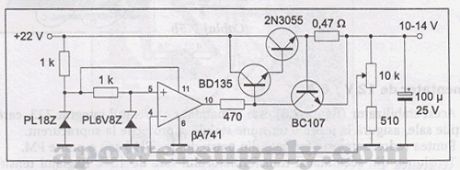
12V Solar Charge Controller Schematic
Bill of Materials
In Excel format (download link at the bottom)
Dropout Voltage
The input voltage exceeds the input voltage by 1.25V when charging at the maximum rate—the lower, the better. Low Dropout Voltage (LDO) is the catch phrase for anything under approximately 2V. This could potentially be reduced to below 1V by making D3 a schottky rectifier.
Current Limiting
Current limiting is provided by the solar panel—it is not a commonly understood fact that the solar panel tends to be a constant current device. For this reason, a solar panel can withstand a short circuit. Therefore, the control does not need current limiting.
Float Charge of Lead-Acid Batteries
This control charges the battery at a constant voltage and also maintains a charged battery (float charge). The float charge voltage specification is a little lower than the charge voltage, so to accommodate both voltages, a compromise is reached by simply reducing the voltage slightly—that is how ALL automotive systems operate. To obtain maximum charge in a 12V battery, set the control to 14 to 14.6V. Automotive systems further reduce voltage to 13 to 13.5V in order to accommodate high temperature operation as the battery is usually located in the hot engine compartment—battery has a negative thermal coefficient of voltage.
Voltage Adjustment
To set the voltage, disconnect the battery and connect a 1K dummy load resistor to the output. The resistor is necessary to shunt potential MOSFET leakage current as well as the green LED current.
LDO Solar Charge Control Circuit Operation
R4 and D1 form a 6V shunt zener voltage reference. Q1 & Q2 make up the classic differential amplifier that amplifies the difference between the reference voltage and the feedback voltage from the arm of potentiometer R6. The output is taken from the collector of Q1 and drives the gate of P Channel MOSFET Q3. Differential voltage gain is probably in the order of 100 to 200. For best performance, I selected Q1 & Q2 for matched hFE. As the feedback voltage increases at the arm of R6, Q2 turns on harder and steals some of the emitter current away from Q1. The collector current of Q1 follows the emitter current and drops less voltage across R1 thus reducing Vgs of Q3 and turning it off. C2 provides frequency compensation to prevent the amplifier from oscillating.
Q3 is dormant unless the battery is connected reverse—should this happen, Q3 turns on and reduces the reference voltage input to zero thus turning Q1 & Q3 and preventing damaging battery current.
D3 prevents the battery voltage from appearing across an inactive solar panel.
Thermal Management
This is a linear series regulator that dissipates significant power when the pass transistor is both conducting current and dropping voltage simultaneously—during maximum charge rate when the voltage drop is low, the heatsink runs warm—when the battery is fully charged and there is low charge current, the heatsink is cold—but when the battery starts to top off at maximum voltage, the heatsink runs very hot—such is the nature of a linear regulator. At 4A, Q3 drops 3.3V (assuming solar panel voltage is 18V)(the remaining 0.7V is the D3 voltage drop. P = 4A * 3.3V = 13.2W. The heatsink is rated at 3.9°C/W, so heatsink temperature rise = 13.2W * 3.9°C/W = 51.5°C. Adding the 25°C ambient temperature results in a heatsink temperature of 76.5°C. While this may seem very HOT to the touch, it is still cool to the transistor that is rated for a junction temperature of 175°C.
For the Future
A 6V version—while this control may be adjusted down to 7V for charging 6V batteries, the performance is marginal, but will function at reduced current. A 6V version is on the drawing board.
Photo
Perf board—sorry, no circuit board artwork at the time of publication. (View)
View full Circuit Diagram | Comments | Reading(1564)
Security Light & Switch with PIR Sensor Update Circuit
Published:2013/11/5 19:09:00 Author:lynne | Keyword: Security Light, Switch

This is a simple update to Mr. Hareendran’s PIR Sensor Security Light circuit. It has a shortcoming limits the relay voltage to approximately 3.3V. While this may function with some 5V relays, it will not function with all. The nature of an emitter follower Darlington forces the output voltage to be two junction drops below the base drive voltage plus a small voltage drop across R1.
In keeping with the spirit of his design, I retained the Darlington arrangement, and the transistor type number – however, I changed the transistors from common collector to common emitter configuration, and connected the relay between the collector output and the positive rail. The relay now utilizes a 12V coil – to use an existing 5V relay, simply add a resistor in series with the coil whose value is scaled up from the coil resistance. Also, I connected the LED across the relay coil rather than powering it via the 2nd relay contact – this way, only one form “C” relay contact is required thus making the relay less expensive – of course it can be done either way. I eliminated some additional, unneeded components.
Security Switch & Light Circuit Schematic
How it works
When motion is detected, the output (pin 2) goes to 5V and current flows through R2 to the base of Q1. The emitter current of Q1 becomes the base current of Q2 – the current gain of a Darlington is the hFE squared or about 10,000 to 50,000 (very high). This easily provides adequate drive current for the relay. R1 provides a means of conducting any potential leakage in Q1 to common and also helps Q2 to turn off faster. D1 is the back diode that circulates the relay coil current when Q1 & Q2 turns off thus preventing a damaging voltage transient.
Testing
No, I did not build and test this one – I just happen to know from experience that this circuit will work OK – if the circuit was new to me, I would definitely Protoboard and test because Murphy may be lurking somewhere. Murphy’s Law states that anything that can go wrong will go wrong… Such is true as I have proven it numerous times.
For the Future
PIR crystal amplifier circuit – yes, it is not difficult.
(View)
View full Circuit Diagram | Comments | Reading(1269)
Programmable Unijunction Transistor Flasher Circuit
Published:2013/11/5 19:07:00 Author:lynne | Keyword: Programmable Unijunction Transistor Flasher

This is simple circuit that illustrates the function of the programmable unijunction transistor. It may be quickly wired on a proto-board.
PUT Flasher Specifications
Flash rate: approx 1hZ
Load current: approx 300uA
Minimum voltage: approx 4V
PUT Flasher Circuit Schematic
How it works
The programmable unijunction transistor remains dormant until the voltage across C1 exceeds the gate voltage of Q1 by one diode drop (0.6V) or in this circuit about 6.8V in reference to circuit common. At this point, current starts to flow into the anode of Q1. When the current exceeds the “peak current” threshold (about 1.25uA), the transistor triggers and shorts all three terminals together until the anode current drops below the “valley current” (about 100uA in this case), and the transistor resets itself. When the transistor triggers, it dumps capacitor C1 across the LED. Peak current is limited by the LED internal resistance.
By varying (programming) the gate voltage, the voltage at which the transistor fires varies—in this case, it varies the flash rate.
Background
This cute little device was developed by General Electric about 50years ago. The original GE part numbers were D13K1 and D13K2 (now 2N6027 and 2N6028). The 2N6028 has tighter specifications for more precision applications. On Semiconductor is now the sole manufacturer, but NTE has a relatively expensive equivalent device.
PUT Applications
There are many, many applications for this device, but it is mainly useful for triggering thyristors. Other than for thyristor triggering, the ubiquitous 555 timer has taken over.
For the Future
Use of this device in a thyristor switch circuit
Bill of Materials
Q1 On Semiconductor 2N6027 (comes only in T0-92 package)
R1 100K
R2 10K
R3 22K
C1 10uF, 25V aluminum electrolytic
D1 LED Red, High Brightness
Battery Standard 9V (View)
View full Circuit Diagram | Comments | Reading(1078)
6V LDO Solar Charge Controller
Published:2013/11/4 20:18:00 Author:lynne | Keyword: LDO Solar Charge Controller
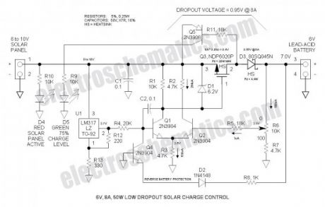
This Low Dropout Voltage (LDO) solar charge controller is a variation of the previously posted 12V LDO controller. It is optimized for charging a 6V lead-acid battery with a 9V solar panel. Minimum voltage drop is less than 1V. It uses a simple differential amplifier and series P channel MOSFET linear regulator. Voltage output is adjustable. It may also be applied in two or four cell lead-acid applications (4V & 8V).It is not recommended for 12V applications.
6 Volt solar charge controller schematic
6V Solar Charge Controller Specifications
Max solar panel rating: 50W (8A, 6V nominal) (open circuit voltage: 9 to 10V)
Output voltage range: 4.7 to 9.8V (adjustable) (not recommended for 12V applications)
Max power dissipation: 16W (includes power dissipation of D3)
Typical dropout voltage: 0.9V @ 8A (less @ lower currents)
Maximum current: 8A (current limiting provided by solar panel characteristics)
Voltage regulation: 80mV (no load to full load)
Battery discharge: 1mA (Chinese controls discharge at typically 5mA)
LED indicators:
RED: Solar panel active
GREEN: Series regulator limiting current (fully charged or topping off)
Reverse battery protection: Control shuts down if battery is inadvertently connected reverse
Operation at lower current/power
While designed for 8A, 50W, it will function just as well at much lower current /power.
LDO Solar Charge Control Photos
Perf board—sorry, no circuit board artwork at the time of publication. (View)
View full Circuit Diagram | Comments | Reading(2471)
555 Low Voltage Operation
Published:2013/11/4 20:17:00 Author:lynne | Keyword: 555 Low Voltage Operation
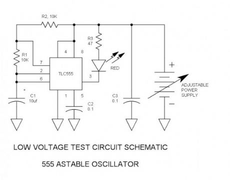
I had heard some stories in the past concerning how poorly the 555 ran below Vcc = 5V, so I embarked on an endeavor to see if I could improve operation. The spec sheet specifies minimum Vcc at 4.5V and I tended to believe it. I set up a simple test circuit and ran each of 5 different bipolar 555 devices while varying Vcc. What I learned surprised me. Not only did it run substantially below 5V, but it ran well. Then I tried a CMOS 555 and that worked below 1V.
555 Test Circuit Schematic
(View)
View full Circuit Diagram | Comments | Reading(960)
AC/DC Microammeter Circuit
Published:2013/11/4 20:16:00 Author:lynne | Keyword: AC/DC Microammeter Circuit

This is a take-off on Mr. Marian’s “Simple Micro Ampere Meter Circuit” that utilizes active circuitry and an analog meter to make sensitive DC current measurements. A reader subsequently asked if it could measure AC microamperes and that is what spawned the idea.
While the schematic is similar, there are notable differences—the voltage drop is now 100mV rather than 1V, the sensitivity is 10nA full scale rather than 100nA and it now measures AC or DC. A precision rectifier rectifies the AC voltage so that a DC meter may be used.
Microammeter Circuit Schematic
(View)
View full Circuit Diagram | Comments | Reading(3678)
Metronome
Published:2013/11/3 20:37:00 Author:lynne | Keyword: Metronome Circuit
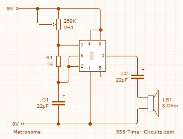
This circuit uses the 555 timer in an Astable operating mode and generates a continuous output via Pin 3 in the form of a square wave. This is then passed through the 22?F electrolytic capacitor to create a smooth oscillation which then creates the 'toc-toc' sound. The speed of the output is controlled by the 250K Potentiometer (VR1). Schematic
Parts List 1x - NE555 Bipolar Timer1x - 1K Resistor (1/4W) 2x - 22?F Electrolytic Capacitor (16V)1x - 250K Potentiometer1x - Loudspeaker (8 Ohm)1x - 9V Voltage Battery (View)
View full Circuit Diagram | Comments | Reading(1094)
MODEL RAILWAY TIME
Published:2013/11/3 20:36:00 Author:lynne | Keyword: MODEL RAILWAY TIME

Here is a circuit that will convert any clock mechanism into Model Railway Time. For those who enjoy model railways, the ultimate is to have a fast clock to match the scale of the layout. This circuit will appear to make time fly by turning the seconds hand once every 6 seconds. The timing can be adjusted by changing the 47k. The electronics in the clock is disconnected from the coil and the circuit drives the coil directly. The circuit takes a lot more current than the original clock (1,000 times more) but this is one way to do the job without a sophisticated chip. (View)
View full Circuit Diagram | Comments | Reading(1104)
MOSQUITO REPELLER
Published:2013/11/3 20:34:00 Author:lynne | Keyword: MOSQUITO REPELLER

This circuit produces a tone above the human audible range and this is supposed to keep the mosquitoes away. You need a piezo diaphragm that will respond to 15kHz and these are very difficult to find.
(View)
View full Circuit Diagram | Comments | Reading(1184)
Single Transistor Amplifier Revisited – Part 3
Published:2013/10/31 22:14:00 Author:lynne | Keyword: Single Transistor, Amplifier
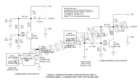
Single Transistor Amplifier Revisited Part 3, Common Base vs Common Emitter Configuration, Update
One nagging question that I have long had is this: How does the common base compare with the common emitter configuration in voltage gain performance? The classic microphone circuit interfaces a loudspeaker (used as microphone) directly to the emitter of a common base amplifier. My initial guess was that the difference would be negligible. However, when I wired and compared the two circuits, I learned a few new things.
Single Transistor Amplifier Schematic
Immediately, I learned that the common base configuration gain was 6db lower than the common emitter. This blew my mind. Then I started checking input resistance and was shocked at how low it measured (8.5Ω). I had previously guessed that it would be about 100Ω. Then I plotted the common base input resistance beside the common emitter input resistance — very useful information. The gain was 6db lower in the common base configuration because the source resistance almost exactly equaled the input resistance.
To obtain reliable input resistance data, I had to reduce the source resistance to 0.1Ω and connect via a Kelvin connection. Input resistance is surprisingly easy to determine experimentally by simply adding a pot between the low impedance voltage source and the amplifier input. Short the resistance and measure AC output voltage. Then increase resistance until the output voltage is exactly half. At this point, the pot resistance equals the input resistance and can be measured by a DMM.
Preface to the update
The initial data was in error due to a near resonant effect in the amplifier—this resonance caused unusually high voltage gain. After correcting the problem, I retook the data and updated the report.
I wish to acknowledge the contribution of Mr. Colin Mitchell who flagged an error regarding coupling capacitor (C1) size. Since this circuit was tested at 1 to 2kHZ, I figured that the capacitor value was not an issue. However, when C1 was increased to 10 uF, the gain unexpectedly decreased. This indicated an additional problem which turned out to be an active filter effect that also involved C2. When C1 and C2 were 0.1uF, the circuit resonated at the 2kHZ test frequency — almost all the elements of a phase shift oscillator were present. This is clear evidence of the veracity of Murphy’s Law — how could all these conditions occur at random?
As a result, Parts 1 and 2 had to be updated as well. (View)
View full Circuit Diagram | Comments | Reading(1223)
Of Wall Warts & Wall Transformers
Published:2013/10/31 22:10:00 Author:lynne | Keyword: Wall Warts, Wall Transformer

With all the recent mania on capacitor limited power adapters at electroschematics.com, the Wall Wart seems to be the neglected power source. Wall warts are small, convenient and have transformer isolation. With line isolation they are free from ground fault shock hazard. The power level and output voltage is ideal for most experimentation, and difficult to specify or obtain “X” capacitors are not required. It has been suggested that wall transformers were coined “wall warts” because they often take up 2 or 3 positions in a power outlet strip, but I say it is simply because they protrude from the wall like a “wart.” The name is simply a humorous alliteration.
Voltage regulation
Voltage regulation (no load to full load) for AC adapters ranges from 12 to 34%. For DC adapters, it is roughly double that or 32 to 80%. This may be seen in the regulation data. The DC adapters have inferior regulation due to the peak detection effect of the input filter capacitor—this is not a serious issue because nothing really operates at no-load, not does anything actually work on AC without rectifiers. For frame of reference (because % regulation tends to be confusing), 0% is perfect and 100% indicates that the voltage drops to half when loaded. Just keep in mind that wall warts tend to be sloppy and the equipment to which it is connected is designed to accept double the specified input voltage safely.
For experimentation, I like the AC versions because I can connect a voltage doubler rectifier to get much higher voltages. Also, if connected to half-wave rectifiers, I can easily obtain ±voltages. (View)
View full Circuit Diagram | Comments | Reading(853)
555 Duty Cycle Control
Published:2013/10/31 22:07:00 Author:lynne | Keyword: 555 Duty Cycle Control

Here is a simple oscillator circuit that varies the duty cycle over a wide range without affecting the frequency. It is a variation of the simple 555 astable oscillator. Initially, I told a reader that there was no standard 555 circuit that could do this, but then the grey matter started working. The use of an air-variable capacitor for frequency control is a mind-blower—nothing short of a time warp!
555 Duty Cycle Control Schematic
Overview
When potentiometer R1 is centered, operation is obvious and the duty cycle is 50%. However, as R1 is rotated in either direction the charge time and discharge times vary accordingly. The two sides of R1 have independent steering diodes (D1 & D2). C1 & C2 make up the timing capacitor. Pins 2 & 6 of the 555 are the upper and lower thresholds of the input comparators. The charge /discharge voltage is taken from pin 3 because it has rail-to-rail voltage swing, and the open collector output (pin 7) cannot do this. The rectangular waveform output is taken from pin 7 instead. R3 is the pull-up resistor.
If constant frequency is desired, C1 could be padded for the correct frequency. However, most experimenters also want variable frequency. Since R1 cannot be varied in total resistance, it cannot vary the frequency. R2 could vary the frequency, but would also affect the duty cycle ratio limits as well. The only practical means of obtaining variable frequency is to vary C1.
Mathematical proof
Q = I * T – where Q is the charge, I is charge current and T is charge time
Q = C * V – where Q is charge, C is capacitance, and V is voltage across the capacitor
∴ I * T = C * V
E = I * R – where E is voltage I is current and R is resistance
∴ I * T = C * I * R – because E is simply another expression for V
T = C * R – dividing by I—we have now proved that charge time is directly proportional to R
So we have a charge resistance and a discharge resistance, the sum of which is constant and equal to the R1 potentiometer total resistance (1 to 3). Therefore, the sum of the charge and discharge times is also constant. Since F = 1/T, the frequency is also be constant.
In other words, the two resistances are complementary and the two time periods are likewise complementary.
The Air Variable Capacitor
The old-fashioned air variable capacitor is old and klunky. While DigiKey offers no such product, these devices remain available on eBay as used or old stock. Every serious experimenter should have one of these. The one I would buy is a 3-gang 440pf. Wired in parallel the total capacitance is 1320pf. Physical size limitations prevent higher capacitances.
Actually, it is fun to play with air variable capacitors.
High impedances
To obtain a reasonably low frequency, R1 had to be selected to have as high a resistance as possible. 2M is the highest value pot I had on hand. A 5M would also be a good selection. To function under such high impedance conditions, I selected the TLC555 CMOS 555. A further advantage of this device is that it has rail-to-rail output voltage—something that the bipolar 555 cannot do.
Limits of accuracy
The accuracy tends to degrade when the slew rate at C1 exceeds about 0.25V/uS. When this happens, the propagation delay of the comparators becomes significant and the frequency drops somewhat. This causes the peaks of the saw-tooth waveform to “skid” past the thresholds before the output switches polarity. This forces the maximum frequency to be lower than about 50kHZ for 50% duty cycle, or lower than 2kHZ with 98% duty cycle. To maintain 1 or 2% frequency accuracy the duty cycle range must drop as frequency increases.
(View)
View full Circuit Diagram | Comments | Reading(1302)
LED DC Voltage Indicator
Published:2013/10/30 21:41:00 Author:lynne | Keyword: LED DC Voltage Indicator


This LED DC voltage indicator circuit is a voltmeter, rather than simply a battery tester. As such it may measure voltages as low as 3V.It utilizes venerable LM741 operational amplifiers applied as comparators that drive LED indicators. Voltage thresholds are 3, 6, 9 and 12V. Above each incremental threshold an additional LED turns on.
DC Voltage Indicator Circuit Schematic
Vcc = 18V
Many voltage indicators rely upon the measurement source voltage for power, but in this voltage indicator case using the LM741, 3V is simply too low for satisfactory operation—the 741 is not specified for low voltage applications. Vcc is higher than what we usually see because it is necessary to have sufficient headroom to bias shunt zener regulator D6. Vcc could have been reduced to 9V by dividing all the threshold reference voltages by a factor of 2, but that would preclude using the LM741 because its input common mode range is specified no lower than 3V from the negative rail—It would definitely not work at 1.5V.
To conserve battery life a “Push to Test” pushbutton switch is used. Another way of doing it would be to use ±9V, and then it could sense voltages down to zero volts if desired. However, this would require the same number of batteries and complicates the pushbutton switch.
Not built or tested
Generally what I submit has been built and tested – this one has not. I have built stuff like this before and used the LM741 as well as the dual version (LM1458), so I have a high degree of confidence that it will work as expected. However, Murphy is always lurking somewhere, just waiting for such an opportunity. The project builder will have the experience of troubleshooting in case it does not function as expected.
Input voltage protection
It is not a good practice to run op amp inputs to the outside world where they would be subject to ESD. R1 and D5 provide the required protection.
D7 protects against accidental reverse battery connection.
Input impedance
Because this dc voltage indicator with LEDs circuit does not derive power from the measurement source, the input impedance is very high. Input impedance is 1M (high but not infinite). In parallel with this is the op amp input bias current that is roughly 4 * 80nA or 320nA. Due to the high impedance, it may be possible to turn on all the LEDs by simply touching the input with your finger. If input noise is an issue, a 0.1uF capacitor across D5 should be helpful.
LED brightness
LED brightness may be varied simply by adjusting the 3.3K series ballast resistor. Most LEDs specify max current to be 20 or 30mA, but efficient green and white versions are blinding at this current so they need much higher value ballast resistors. (View)
View full Circuit Diagram | Comments | Reading(1502)
TL497A Voltage Converter
Published:2013/10/30 21:38:00 Author:lynne | Keyword: Voltage Converter

This voltage converter is built with TL497A and converts an input voltage of 5…12 voltage to a higher level of 15…30 volts. This is specially helpful in mobile applications where power supply levels are commonly limited to 12 volts supplied by batteries.The voltage converter circuit uses the TL497A as a flyback-voltage converter. The choke coil is 40uH/2A. Capacitors C2 annd C1 suppress voltage spikes. The maximum output current depends on the difference between the input and the output voltages and is around 100mA. The ripple voltage is relatively low. The standby current is around 8mA and the efficiency is about 70%.
TL497A voltage converter circuit diagram
(View)
View full Circuit Diagram | Comments | Reading(2248)
3V to 24V Variable Power Supply
Published:2013/10/30 21:36:00 Author:lynne | Keyword: Power Supply

This 3V to 24 volt variable-regulated power supply can be adjusted from 3 to 25 volts and is current limited to 2 amps as shown, but may be increased to 3 amps or more by selecting a smaller current sense resistor (0.3 ohm). The 2N3055 and 2N3053 transistors should be mounted on suitable heat sinks and the current sense resistor should be rated at 3 watts or more.
Voltage regulation is controlled by 1/2 of a 1558 or 1458 op-amp. The 1458 may be substituted in the circuit below, but it is recommended the supply voltage to pin 8 be limited to 30 VDC, which can be accomplished by adding a 6.2 volt zener or 5.1 K resistor in series with pin 8. The maximum DC supply voltage for the 1458 and 1558 is 36 and 44 respectively. The power transformer should be capable of the desired current while maintaining an input voltage at least 4 volts higher than the desired output, but not exceeding the maximum supply voltage of the op-amp under minimal load conditions.
The power transformer shown is a center tapped 25.2 volt AC / 2 amp unit that will provide regulated outputs of 24 volts at 0.7 amps, 15 volts at 2 amps, or 6 volts at 3 amps. The 3 amp output is obtained using the center tap of the transformer with the switch in the 18 volt position. All components should be available at Radio Shack with the exception of the 1558 op-amp.
Variable Power Supply Circuit Diagram
(View)
View full Circuit Diagram | Comments | Reading(1760)
Power Supply Monitor for TTL
Published:2013/10/29 21:03:00 Author:lynne | Keyword: Power Supply Monitor
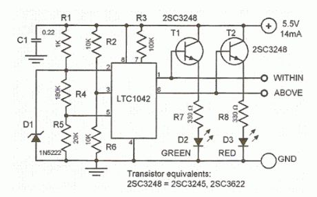
This simple TTL power supply monitor circuit monitors the 5-volt level TTL power line and gives a signal whether the supply voltage is outside or within the necessary range or “window”. The heart of thepower supply monitoris a low-current integrated window comparator. The center of this window is set at 2.5 volt +/- 0.005 volt by the bandgap reference diode D1 which is connected to pin 2 of LTC1042. The width of this window must be 20% (+/- 10%) of the reference voltage.The reference voltage is reduced by 25% through R4 and R5 and fed to pin 5 of the IC. The monitored voltage is then fed to pin 2 so that the green LED D2 will light up when the voltage is within the desired range. Otherwise, the red LED D3 will light up signalling that the voltage is out of range.
TTL power supply monitor circuit diagram
(View)
View full Circuit Diagram | Comments | Reading(1087)
LM2678 Voltage Regulator Circuit
Published:2013/10/29 20:49:00 Author:lynne | Keyword: Voltage Regulator Circuit


The LM2678 series of regulators are monolithic integrated circuits for a step-down switching voltage regulator capable of driving up to 5A loads with excellent line and load regulation characteristics. High efficiency (>90%) is obtained through the use of a low ON-resistance DMOS power switch. The series consists of fixed output voltages of 3.3V, 5V and 12V and an adjustable output version.
LM2678 12vdc 5amp voltage regulator schematic
LM2678 features
Efficiency up to 92%
Simple and easy to design with (using off-the-shelf external components)
120 mΩ DMOS output switch
3.3V, 5V and 12V fixed output and adjustable (1.2V to 37V ) versions
50μA standby current when switched OFF
±2%maximum output tolerance over full line and load conditions
Wide input voltage range: 8V to 40V
260 KHz fixed frequency internal oscillator
LM2678 applications
Simple to design, high efficiency (>90%) step-down switching voltage regulators
Efficient system pre-regulator for linear voltage regulators
Battery chargers (View)
View full Circuit Diagram | Comments | Reading(1113)
Engine Running Detector, Load Switch
Published:2013/10/29 20:40:00 Author:lynne | Keyword: Engine Running Detector, Load Switch
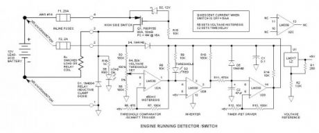
This circuit determines when an engine is running, and when running, it turns on a solid-state switch to automatically power accessories. It does this simply by measuring battery voltage—when not charging, battery voltage is less than approx. 13.2V—when charging, it is greater than approx. 14.0V. Seems like a simple task, does it not? If so, why are there not already devices available to do this seemingly simple task?
While the concept is simple, there are numerous problems involved as follows:
Voltage must be sensed as close to the battery as possible, and voltage sense wiring must be separate from power wiring—hence the requirement for the Kelvin connection. This is why I wrote the recent article:What is a Kelvin Connection?
Since this circuit is connected directly to the battery, circuit protection is absolutely essential. This is why I wrote the recent article:Low Voltage & Automotive Circuit Protection.
Voltage threshold must be accurate—requires stable voltage reference.
Circuit must have hysteresis for positive switching.
Load switch must have substantial delay to prevent unintended or nuisance switching.
Quiescent current must be low to prevent battery discharge.
Charging system must function correctly—alternator must float charge the battery as well as power all connected accessories when engine is at idle speed.
Due to variations in battery charging voltage in different systems and a relatively narrow voltage threshold window, there is no one size fits all voltage setting. As a result, the threshold must be adjustable.
Due to these complexities, this circuit is not recommended for the novice. However, if installed using proper circuit protection & wiring practices, the only failure mode is unintended battery discharge should it not automatically disconnect the load.
(View)
View full Circuit Diagram | Comments | Reading(1574)
Simple 12V DC Power Supply Circuits
Published:2013/10/28 20:23:00 Author:lynne | Keyword: Power Supply Circuit


Here are 4 simple 12V power supply circuits with output voltages around 12V. First power supply circuit is built with BD139, one zener diode and a few passive components. Each of the schematic is very simple to construct and will function without problems if you respect the maximum power supply ratings.
12V dc power supply schematics
12V BD139 power supply circuit
LM7812 power supply schematic
A very simple PS circuit with the basic 3 Amper version of LM7812 IC.
LM317 variable power supply circuit
2N3055 adjustable power supply schematic
This power supply circuit has a over-current protection and a good stabilized voltage. It can deliver up to 1.6 A.
(View)
View full Circuit Diagram | Comments | Reading(2454)
Capacitor Input Filter Calculation
Published:2013/10/28 20:20:00 Author:lynne | Keyword: Capacitor Input Filter
This is a simple means of calculating the required size of the input filter capacitor in a basic power supply, or calculating the peak-to-peak ripple voltage in an existing supply. It works by assuming that the capacitor supplies current to the load approximately 70% of the cycle—the remaining 30% is supplied directly by the rectified voltage and during this period the capacitor is charged as well.
Graphic
(View)
View full Circuit Diagram | Comments | Reading(1117)
| Pages:54/2234 At 204142434445464748495051525354555657585960Under 20 |
Circuit Categories
power supply circuit
Amplifier Circuit
Basic Circuit
LED and Light Circuit
Sensor Circuit
Signal Processing
Electrical Equipment Circuit
Control Circuit
Remote Control Circuit
A/D-D/A Converter Circuit
Audio Circuit
Measuring and Test Circuit
Communication Circuit
Computer-Related Circuit
555 Circuit
Automotive Circuit
Repairing Circuit