Amplifier Circuit
Single Transistor Amplifier Revisited – Part 3
Published:2013/10/31 22:14:00 Author:lynne | Keyword: Single Transistor, Amplifier | From:SeekIC

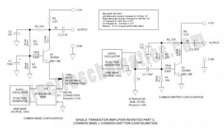
Single Transistor Amplifier Revisited Part 3, Common Base vs Common Emitter Configuration, Update
One nagging question that I have long had is this: How does the common base compare with the common emitter configuration in voltage gain performance? The classic microphone circuit interfaces a loudspeaker (used as microphone) directly to the emitter of a common base amplifier. My initial guess was that the difference would be negligible. However, when I wired and compared the two circuits, I learned a few new things.
Single Transistor Amplifier Schematic
Immediately, I learned that the common base configuration gain was 6db lower than the common emitter. This blew my mind. Then I started checking input resistance and was shocked at how low it measured (8.5Ω). I had previously guessed that it would be about 100Ω. Then I plotted the common base input resistance beside the common emitter input resistance — very useful information. The gain was 6db lower in the common base configuration because the source resistance almost exactly equaled the input resistance.
To obtain reliable input resistance data, I had to reduce the source resistance to 0.1Ω and connect via a Kelvin connection. Input resistance is surprisingly easy to determine experimentally by simply adding a pot between the low impedance voltage source and the amplifier input. Short the resistance and measure AC output voltage. Then increase resistance until the output voltage is exactly half. At this point, the pot resistance equals the input resistance and can be measured by a DMM.
Preface to the update
The initial data was in error due to a near resonant effect in the amplifier—this resonance caused unusually high voltage gain. After correcting the problem, I retook the data and updated the report.
I wish to acknowledge the contribution of Mr. Colin Mitchell who flagged an error regarding coupling capacitor (C1) size. Since this circuit was tested at 1 to 2kHZ, I figured that the capacitor value was not an issue. However, when C1 was increased to 10 uF, the gain unexpectedly decreased. This indicated an additional problem which turned out to be an active filter effect that also involved C2. When C1 and C2 were 0.1uF, the circuit resonated at the 2kHZ test frequency — almost all the elements of a phase shift oscillator were present. This is clear evidence of the veracity of Murphy’s Law — how could all these conditions occur at random?
As a result, Parts 1 and 2 had to be updated as well.
Reprinted Url Of This Article:
http://www.seekic.com/circuit_diagram/Amplifier_Circuit/Single_Transistor_Amplifier_Revisited_–_Part_3.html
Print this Page | Comments | Reading(3)

Article Categories
power supply circuit
Amplifier Circuit
Basic Circuit
LED and Light Circuit
Sensor Circuit
Signal Processing
Electrical Equipment Circuit
Control Circuit
Remote Control Circuit
A/D-D/A Converter Circuit
Audio Circuit
Measuring and Test Circuit
Communication Circuit
Computer-Related Circuit
555 Circuit
Automotive Circuit
Repairing Circuit
Code: