
Circuit Diagram
Index 57
7447 pin configuration
Published:2013/10/9 19:56:00 Author:lynne | Keyword: 7447 pin configuration
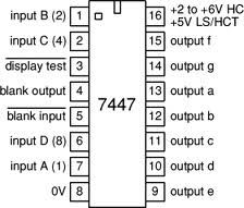
According to the 7447 datasheet the 7446A and 7447A ICs feature active-low outputs designed for driving common-anode LEDs or incandescent indicators directly. All of the circuits have full ripple-blanking input/output controls and a lamp test input. Segment identification and resultant displays are shown on a following page.
Display patterns for BCD input counts above nine are unique symbols to authenticate input conditions. All of the circuits incorporate automatic leading and/or trailing-edge, zero-blanking control (RBI and RBO). Lamp test (LT) of these devices may be performed at any time when the BI/RBO node is at a high logic level. All types contain an overriding blanking input (BI) which can be used to control the lamp intensity (by pulsing) or to inhibit the outputs.
7447 Datasheet Features
All circuit types feature lamp intensity modulation capability
Open-collector outputs drive indicators directly
Lamp-test provision
Leading/trailing zero suppression (View)
View full Circuit Diagram | Comments | Reading(2281)
24V to 36V Battery Charger
Published:2013/10/9 19:55:00 Author:lynne | Keyword: 24V to 36V Battery Charger
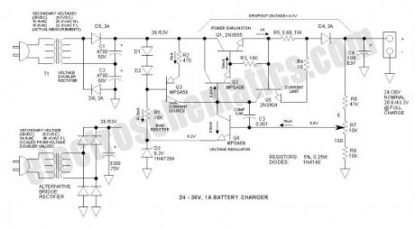
This 24V to 36V linear battery charger is long overdue. While this is an old circuit technique, it is optimized for charging higher voltage lead-acid battery packs, and could be used on other types of batteries as well. By proper transformer selection, it can be optimized for either 24 or 36V. Note that actual float charge voltage requires 2.4V /cell or 28.8 & 43.2V @ full charge respectively. (View)
View full Circuit Diagram | Comments | Reading(1460)
TDA2003 Audio Amplifier Circuits
Published:2013/10/9 19:53:00 Author:lynne | Keyword: TDA2003 Audio Amplifier Circuits


TDA2003 is a cheap amplifier that is designed to run on single rail power supplies (unipolar). It provides a high output current capability (up to 3.5A), very low harmonic and cross-over distortion.TDA2003 10W car radio audio amplifier
TDA2003 18W bridged audio amplifier
TDA2003 can be used as an BCL (bridged amplifier) and car deliver up to 18W.
(View)
View full Circuit Diagram | Comments | Reading(2045)
TDA2005 Audio Amplifier Circuits
Published:2013/10/8 20:17:00 Author:lynne | Keyword: TDA2005 Audio Amplifier Circuits
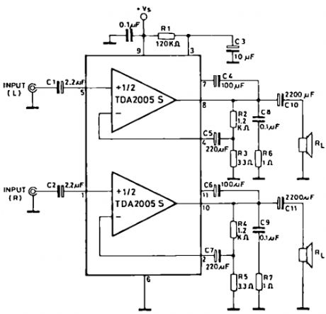
TDA2005 is a class B dual audio power amplifier specifically designed for car radio applications. Its high current capability (up to 3.5 A) and the ability to drive very low impedance loads (down to 1.6 ohms) makes this circuit a good choice for cheap power booster amplifiers. (View)
View full Circuit Diagram | Comments | Reading(1412)
TDA2030 Audio Amplifier Circuits
Published:2013/10/8 20:16:00 Author:lynne | Keyword: TDA2030 Audio Amplifier Circuits

TDA2030 is a monolithic integrated circuit in Pentawatt package, intended for use as a low frequency class AB amplifier. It provides 14W output power (d = 0.5%) at 14V/4Ω at ± 14V or 28V, the guaranteed output power is 12W on a 4Ω load or 8W on a 8Ω
TDA2030 10W audio amplifier circuit
TDA 2030 audio amplifier can output 20 W but in this schematic we have reduced the power to 10W and we use 10w speakers.
(View)
View full Circuit Diagram | Comments | Reading(1374)
TDA7294 Audio Amplifier Circuits
Published:2013/10/8 20:14:00 Author:lynne | Keyword: TDA7294 Audio Amplifier Circuits
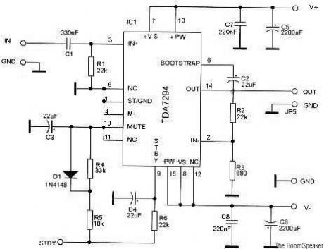
TDA7294 is a monolithic integrated circuit in Multiwatt15 package, with high output power (up to 100W) intended for use as audio class AB amplifier in Hi-Fi field applications (Home Stereo, self powered loudspeakers, Topclass TV). Thanks to the wide voltage range and to the high out current capability it is able to supply the highest power into both 4W and 8W loads even in presence of poor supply regulation, with high Supply Voltage Rejection. (View)
View full Circuit Diagram | Comments | Reading(1537)
Arduino Uno Pinout
Published:2013/10/7 22:12:00 Author:lynne | Keyword: Arduino Uno Pinout
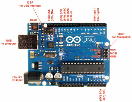
Input and Output
Each of the 14 digital pins on the Arduino Uno can be used as an input or output, using pinMode(), digitalWrite(), and digitalRead() functions. They operate at 5 volts. Each pin can provide or receive a maximum of 40 mA and has an internal pull-up resistor (disconnected by default) of 20-50 kOhms.In addition, some pins have specialized functions:Serial: pins 0 (RX) and 1 (TX). Used to receive (RX) and transmit (TX) TTL serial data. These pins are connected to the corresponding pins of the ATmega8U2 USB-to-TTL Serial chip.
External Interrupts: pins 2 and 3. These pins can be configured to trigger an interrupt on a low value, a rising or falling edge, or a change in value. See the attachInterrupt() function for details.
PWM: 3, 5, 6, 9, 10, and 11. Provide 8-bit PWM output with the analogWrite() function.
SPI: 10 (SS), 11 (MOSI), 12 (MISO), 13 (SCK). These pins support SPI communication using the SPI library.
LED: 13. There is a built-in LED connected to digital pin 13. When the pin is HIGH value, the LED is on, when the pin is LOW, it’s off.
The Uno has 6 analog inputs, labeled A0 through A5, each of which provide 10 bits of resolution (i.e. 1024 different values). By default they measure from ground to 5 volts, though is it possible to change the upper end of their range using the AREF pin and the analogReference() function. Additionally, some pins have specialized functionality:
TWI: A4 or SDA pin and A5 or SCL pin. Support TWI communication using the Wire library.
There are a couple of other pins on the board:
AREF. Reference voltage for the analog inputs. Used with analogReference().
Reset. Bring this line LOW to reset the microcontroller. Typically used to add a reset button to shields which block the one on the board. (View)
View full Circuit Diagram | Comments | Reading(1126)
Arduino Leonardo Pinout
Published:2013/10/7 22:05:00 Author:lynne | Keyword: Arduino Leonardo Pinout
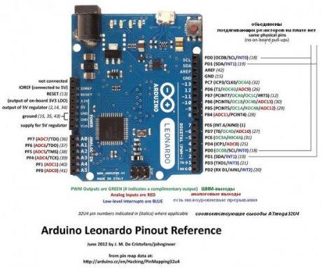
Input and Output
Each of the 20 digital i/o pins on the Arduino Leonardo can be used as an input or output, using pinMode(), digitalWrite(), and digitalRead() functions. They operate at 5 volts. Each pin can provide or receive a maximum of 40 mA and has an internal pull-up resistor (disconnected by default) of 20-50 kOhms.In addition, some pins have specialized functions:Serial: 0 (RX) and 1 (TX). Used to receive (RX) and transmit (TX) TTL serial data using the ATmega32U4 hardware serial capability. Note that on the Leonardo, the Serial class refers to USB (CDC) communication; for TTL serial on pins 0 and 1, use the Serial1 class.
TWI: 2 (SDA) and 3 (SCL). Support TWI communication using the Wire library.External Interrupts: 2 and 3. These pins can be configured to trigger an interrupt on a low value, a rising or falling edge, or a change in value. See the attachInterrupt() function for details.
PWM: 3, 5, 6, 9, 10, 11, and 13. Provide 8-bit PWM output with the analogWrite() function.
SPI: on the ICSP header. These pins support SPI communication using the SPI library. Note that the SPI pins are not connected to any of the digital I/O pins as they are on the Uno, They are only available on the ICSP connector. This means that if you have a shield that uses SPI, but does NOT have a 6-pin ICSP connector that connects to the Leonardo’s 6-pin ICSP header, the shield will not work.
LED: 13. There is a built-in LED connected to digital pin 13. When the pin is HIGH value, the LED is on, when the pin is LOW, it’s off.
Analog Inputs: A0-A5, A6 – A11 (on digital pins 4, 6, 8, 9, 10, and 12). The Leonardo has 12 analog inputs, labeled A0 through A11, all of which can also be used as digital i/o. Pins A0-A5 appear in the same locations as on the Uno; inputs A6-A11 are on digital i/o pins 4, 6, 8, 9, 10, and 12 respectively. Each analog input provide 10 bits of resolution (i.e. 1024 different values). By default the analog inputs measure from ground to 5 volts, though is it possible to change the upper end of their range using the AREF pin and the analogReference() function.
There are a couple of other pins on the board:
AREF. Reference voltage for the analog inputs. Used with analogReference().Reset. Bring this line LOW to reset the microcontroller. Typically used to add a reset button to shields which block the one on the board. (View)
View full Circuit Diagram | Comments | Reading(1237)
Arduino Due Pinout
Published:2013/10/7 22:04:00 Author:lynne | Keyword: Arduino Due Pinout
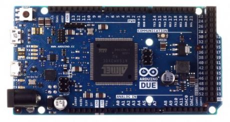
Input and Output
Digital I/O: pins from 0 to 53
Each of the 54 digital pins on the Due can be used as an input or output, using pinMode(), digitalWrite(), and digitalRead() functions. They operate at 3.3 volts. Each pin can provide (source) a current of 3 mA or 15 mA, depending on the pin, or receive (sink) a current of 6 mA or 9 mA, depending on the pin. They also have an internal pull-up resistor (disconnected by default) of 100 KOhm.In addition, some pins have specialized functions:Serial: 0 (RX) and 1 (TX)Serial 1: 19 (RX) and 18 (TX)Serial 2: 17 (RX) and 16 (TX)Serial 3: 15 (RX) and 14 (TX)
Used to receive (RX) and transmit (TX) TTL serial data (with 3.3 V level). Pins 0 and 1 are connected to the corresponding pins of the ATmega16U2 USB-to-TTL Serial chip.
PWM: Pins 2 to 13
Provide 8-bit PWM output with the analogWrite() function. the resolution of the PWM can be changed with the analogWriteResolution() function.
SPI: SPI header (ICSP header on other Arduino boards)
These pins support SPI communication using the SPI library. The SPI pins are broken out on the central 6-pin header, which is physically compatible with the Uno, Leonardo and Mega2560. The SPI header can be used only to communicate with other SPI devices, not for programming the SAM3X with the In-Circuit-Serial-Programming technique. The SPI of the Due has also advanced features that can be used with the Extended SPI methods for Due.
CAN: CANRX and CANTX
These pins support the CAN communication protocol but are not not yet supported by Arduino APIs.
“L” LED: 13
There is a built-in LED connected to digital pin 13. When the pin is HIGH, the LED is on, when the pin is LOW, it’s off. It is also possible to dim the LED because the digital pin 13 is also a PWM outuput.
TWI 1: 20 (SDA) and 21 (SCL)TWI 2: SDA1 and SCL1.
Support TWI communication using the Wire library.
Analog Inputs: pins from A0 to A11
The Due has 12 analog inputs, each of which can provide 12 bits of resolution (i.e. 4096 different values). By default, the resolution of the readings is set at 10 bits, for compatibility with other Arduino boards. It is possible to change the resolution of the ADC with analogReadResolution(). The Due’s analog inputs pins measure from ground to a maximum value of 3.3V. Applying more then 3.3V on the Due’s pins will damage the SAM3X chip. The analogReference() function is ignored on the Due.The AREF pin is connected to the SAM3X analog reference pin through a resistor bridge. To use the AREF pin, resistor BR1 must be desoldered from the PCB.
DAC1 and DAC2
These pins provides true analog outputs with 12-bits resolution (4096 levels) with the analogWrite() function. These pins can be used to create an audio output using the Audio library.
Other pins on the board:AREF Reference voltage for the analog inputs. Used with analogReference().
Reset Bring this line LOW to reset the microcontroller. Typically used to add a reset button to shields which block the one on the board. (View)
View full Circuit Diagram | Comments | Reading(1139)
Arduino Mega 2560 Pinout
Published:2013/9/29 20:01:00 Author:lynne | Keyword: Arduino Mega 2560 Pinout
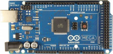
Input and Output
Each of the 54 digital pins on the Arduino 2560 Mega can be used as an input or output, using pinMode(), digitalWrite(), and digitalRead() functions. They operate at 5 volts. Each pin can provide or receive a maximum of 40 mA and has an internal pull-up resistor (disconnected by default) of 20-50 kOhms.In addition, some pins have specialized functions:Serial: 0 (RX) and 1 (TX);Serial 1: 19 (RX) and 18 (TX);Serial 2: 17 (RX) and 16 (TX);Serial 3: 15 (RX) and 14 (TX).
Used to receive (RX) and transmit (TX) TTL serial data. Pins 0 and 1 are also connected to the corresponding pins of the ATmega16U2 USB-to-TTL Serial chip.
External Interrupts: 2 (interrupt 0), 3 (interrupt 1), 18 (interrupt 5), 19 (interrupt 4), 20 (interrupt 3), and 21 (interrupt 2). These pins can be configured to trigger an interrupt on a low value, a rising or falling edge, or a change in value. See the attachInterrupt() function for details.
PWM: 2 to 13 and 44 to 46. Provide 8-bit PWM output with the analogWrite() function.SPI: 50 (MISO), 51 (MOSI), 52 (SCK), 53 (SS). These pins support SPI communication using the SPI library. The SPI pins are also broken out on the ICSP header, which is physically compatible with the Uno, Duemilanove and Diecimila.
LED: 13. There is a built-in LED connected to digital pin 13. When the pin is HIGH value, the LED is on, when the pin is LOW, it’s off.
TWI: 20 (SDA) and 21 (SCL). Support TWI communication using the Wire library. Note that these pins are not in the same location as the TWI pins on the Duemilanove or Diecimila.The Mega2560 has 16 analog inputs, each of which provide 10 bits of resolution (i.e. 1024 different values). By default they measure from ground to 5 volts, though is it possible to change the upper end of their range using the AREF pin and analogReference() function.
There are a couple of other pins on the board:
AREF. Reference voltage for the analog inputs. Used with analogReference().Reset. Bring this line LOW to reset the microcontroller. Typically used to add a reset button to shields which block the one on the board. (View)
View full Circuit Diagram | Comments | Reading(1693)
Arduino Mega ADK Pinout
Published:2013/9/29 20:00:00 Author:lynne | Keyword: Arduino Mega ADK Pinout
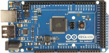
Input and Output
Each of the 50 digital pins on the Arduino Mega ADK can be used as an input or output, using pinMode(), digitalWrite(), and digitalRead() functions. They operate at 5 volts. Each pin can provide or receive a maximum of 40 mA and has an internal pull-up resistor (disconnected by default) of 20-50 kOhms.In addition, some pins have specialized functions:Serial: 0 (RX) and 1 (TX);Serial 1: 19 (RX) and 18 (TX);Serial 2: 17 (RX) and 16 (TX);Serial 3: 15 (RX) and 14 (TX).
Used to receive (RX) and transmit (TX) TTL serial data. Pins 0 and 1 are also connected to the corresponding pins of the ATmega8U2 USB-to-TTL Serial chip.
External Interrupts: 2 (interrupt 0), 3 (interrupt 1), 18 (interrupt 5), 19 (interrupt 4), 20 (interrupt 3), and 21 (interrupt 2). These pins can be configured to trigger an interrupt on a low value, a rising or falling edge, or a change in value. See the attachInterrupt() function for details.
PWM: 2 to 13 and 44 to 46. Provide 8-bit PWM output with the analogWrite() function.
SPI: 50 (MISO), 51 (MOSI), 52 (SCK), 53 (SS). These pins support SPI communication using the SPI library. The SPI pins are also broken out on the ICSP header, which is physically compatible with the Uno, Duemilanove and Diecimila.
USB Host: MAX3421E. The MAX3421E comunicate with Arduino with the SPI bus. So it uses the following pins:Digital: 7 (RST), 50 (MISO), 51 (MOSI), 52 (SCK).
NB: Please do not use Digital pin 7 as input or output because is used in the comunication with MAX3421E
Non broken out on headers: PJ3 (GP_MAX), PJ6 (INT_MAX), PH7 (SS).
LED: 13. There is a built-in LED connected to digital pin 13. When the pin is HIGH value, the LED is on, when the pin is LOW, it’s off.
TWI: 20 (SDA) and 21 (SCL). Support TWI communication using the Wire library. Note that these pins are not in the same location as the TWI pins on the Duemilanove or Diecimila.
The ADK has 16 analog inputs, each of which provide 10 bits of resolution (i.e. 1024 different values). By default they measure from ground to 5 volts, though is it possible to change the upper end of their range using the AREF pin and analogReference() function.
There are a couple of other pins on the board:
AREF. Reference voltage for the analog inputs. Used with analogReference().
Reset. Bring this line LOW to reset the microcontroller. Typically used to add a reset button to shields which block the one on the board. (View)
View full Circuit Diagram | Comments | Reading(987)
Arduino Ethernet Pinout
Published:2013/9/29 19:59:00 Author:lynne | Keyword: Arduino Ethernet Pinout
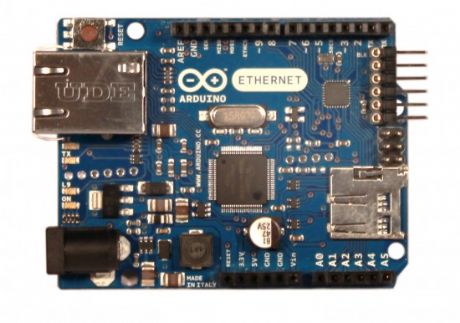
Input and Output
Each of the 14 digital pins on the Ethernet board can be used as an input or output, using pinMode(), digitalWrite(), and digitalRead() functions. They operate at 5 volts. Each pin can provide or receive a maximum of 40 mA and has an internal pull-up resistor (disconnected by default) of 20-50 kOhms.In addition, some pins have specialized functions:Serial: 0 (RX) and 1 (TX). Used to receive (RX) and transmit (TX) TTL serial data.
External Interrupts: 2 and 3. These pins can be configured to trigger an interrupt on a low value, a rising or falling edge, or a change in value. See the attachInterrupt() function for details.
PWM: 3, 5, 6, 9, and 10. Provide 8-bit PWM output with the analogWrite() function.
SPI: 10 (SS), 11 (MOSI), 12 (MISO), 13 (SCK). These pins support SPI communication using the SPI library.
LED: 9. There is a built-in LED connected to digital pin 9. When the pin is HIGH value, the LED is on, when the pin is LOW, it’s off. On most other arduino boards, this LED is found on pin 13. It is on pin 9 on the Ethernet board because pin 13 is used as part of the SPI connection.
The Ethernet board has 6 analog inputs, labeled A0 through A5, each of which provide 10 bits of resolution (i.e. 1024 different values). By default they measure from ground to 5 volts, though is it possible to change the upper end of their range using the AREF pin and the analogReference() function. Additionally, some pins have specialized functionality:
TWI: A4 (SDA) and A5 (SCL). Support TWI communication using the Wire library.
There are a couple of other pins on the board:
AREF. Reference voltage for the analog inputs. Used with analogReference().
Reset. Bring this line LOW to reset the microcontroller. Typically used to add a reset button to shields which block the one on the board.v (View)
View full Circuit Diagram | Comments | Reading(945)
Arduino Pinout
Published:2013/9/28 21:10:00 Author:lynne | Keyword: Arduino Pinout


I myself own an Arduino Uno R3 and found that it can simplify my projects development and microcontroller programming, but sometimes I need to know the Arduino pinout. That is why I have written this article. There are many arduino boards with different pinouts. We will start with my favorite: Arduino Uno.
(View)
View full Circuit Diagram | Comments | Reading(1690)
Automatic Door Light Switch
Published:2013/9/28 21:08:00 Author:lynne | Keyword: Automatic Door Light Switch

This automatic door light switch circuit turns ON a lamp when a door is opened then turns it OFF when the door is opened again. The working principle of the light switch is quite simple. The bistables inside CMOS 4013 are conected in series. FF2 is configured as a R-S memory to store the state of the switch. S1 must switch as soon as the door opens that is why it will be mounted on the door jamb.
When the door will be opened FF2 is registered and its output (pin 13) will be 1.This output, connected at the tact entry of FF1 (pin 3) will open T1 and activate the relay switching ON the light.
When the door is closed nothing will happen because FF2 is unregistered and its output (pin 13) passes in state “0″. Only when the door is opened again, FF1 will change its state and the output at pin 1 will block the transistor so the relay will be disconnected and the door light switch turns off the lamp.The relay must operate at voltages between 5 V and 15 V.
(View)
View full Circuit Diagram | Comments | Reading(1663)
LM2903, LM393 Datasheet
Published:2013/9/28 21:07:00 Author:lynne | Keyword: LM2903, LM393 Datasheet
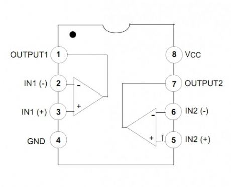
The LM2903, LM393/LM393A, LM293A consist of two independent voltage comparators designed to operate from a single power supply over a wide voltage range.LM393, LM2903 Features
Single Supply Operation: 2V to 36V
Dual Supply Operation: ±1V to ±18V
Allow Comparison of Voltages Near Ground Potential
Low Current Drain 800µA Typ.
Compatible with all Forms of Logic
Low Input Bias Current 25nA Typ.
Low Input Offset Current ±5nA Typ.
Low Offset Voltage ±1mV Typ.
(View)
View full Circuit Diagram | Comments | Reading(1553)
Vibration Impulse Counter
Published:2013/9/26 20:25:00 Author:lynne | Keyword: Vibration Impulse Counter
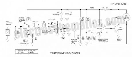
This is a take off from the previously posted bicycle anti-theft alarm. One commenter indicated a desire to adapt it to a threshold step plate vibration detector to count patrons entering a place of business. The circuit is now adapted for that application. Note that there are a myriad of other applications for this circuit.It consists of a piezoelectric film transducer, charge amplifier, charge pump detector, Schmitt trigger and counter driver. (View)
View full Circuit Diagram | Comments | Reading(1058)
LM3915 Circuit
Published:2013/9/26 20:24:00 Author:lynne | Keyword: LM3915 Circuit
The LM3915 datasheet specifies that the IC is a monolithic integrated circuit that senses analog voltage levels and drives ten LEDs, LCDs or vacuum fluorescent displays, providing a logarithmic 3 dB/step analog display. One pin changes the display from a bar graph to a moving dot display. LED current drive is regulated and programmable, eliminating the need for current limiting resistors. The whole display system can operate from a single supply as low as 3V or as high as 25V.
LM3915 Features
3 dB/step, 30 dB range
Drives LEDs, LCDs, or vacuum fluorescents
Bar or dot display mode externally selectable by user
Expandable to displays of 90 dB
Internal voltage reference from 1.2V to 12V
Operates with single supply of 3V to 25V
Inputs operate down to ground
Output current programmable from 1 mA to 30 mA
Input withstands ±35V without damage or false outputs
Outputs are current regulated, open collectors
Directly drives TTL or CMOS
The internal 10-step divider is floating and can be referenced to a wide range of voltages (View)
View full Circuit Diagram | Comments | Reading(1129)
Photoelectric Smoke Detector
Published:2013/9/26 20:22:00 Author:lynne | Keyword: Photoelectric Smoke Detector
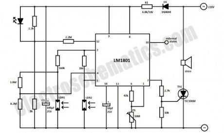

This photoelectric smoke detector circuit uses one LED and 2 LDRs to detect the smoke and sound an alarm. The LM1801 IC is the best choice for this circuit because we need a few external components and is used in almost any smoke alarm.
The whole photoelectric smoke detector circuit is powered from the 220V mains supply. D1 regulates the voltage, R1 decreases it until a proper level for the IC. C1 capacitor is filtering this voltage that is then stabilized with the zener diode inside LM1801.
Physically, the LDRs must be installed so that the smoke particles reflects the light from the LED on LDR2, causing decrease in its resistance. When there is smoke between the LED and LDRs the IC switches the thyristor Th1 which activates the siren.
The most difficult part in constructing this photoelectric smoke detector is to placement of LED and LDRs. Basically, the LED must be positioned exactly midway between the 2 LDRs, making sure there is no air flow between LED and LDR1. This can be accomplished by placing a transparent box around LDR1 and LED.The whole circuit sensitivity is adjustable with P1.
(View)
View full Circuit Diagram | Comments | Reading(1244)
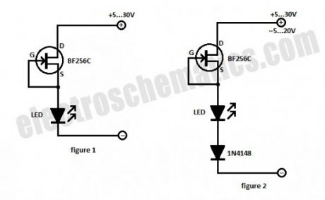
Wide Voltage Range LED
Published:2013/9/25 20:08:00 Author:lynne | Keyword: Wide Voltage Range LED

LEDs are well-known for their current consumption, and sometimes a resistor is necessary to limit the current at a moderate value, between 10 to 30 mA.This solution has a drawback, because the value of the resistor must be calculated for each value of voltage.
Replacing the resistor with a FET transistor offers a number of advantages (figure 1). By shorting the gate with source, the transistor forms o current source without requiring additional components. In this case BF256C is used and its constant current is between 11 mA and 15 mA when the voltage is between 5 V to 30 V.
You may use a universal diode like 1N4148 to ensure polarity protection of the LED (figure 2). As a result, the LED can be powered with AC voltages between 5 V and 20 V. At the frequency of 50 Hz the LED is slightly flashing (not quite noticeable) reducing its brightness because of the half-wave rectification.
(View)
View full Circuit Diagram | Comments | Reading(1420)
DIY Solar Tracker System
Published:2013/9/25 20:07:00 Author:lynne | Keyword: DIY Solar Tracker System

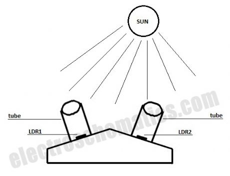
The solar panels are operating at optimal parameters when they are at the perfect right angle to the sun. Unfortunately this is accomplished only if solar panels are rotated by the sun. This is the purpose of this diy solar tracker system.
The solar tracker circuit uses a window comparator to maintain the motor in a idle state as long as the two LDRs are under the same illumination level. In this case, half the voltage is applied to the noninverting input of A1 and to the inverting input of A1.
solar tracking components
T1, T3 = BD239, BD139
T2, T4 = BD240, BD140
A1, A2 = 1/2 of LM324
Diodes = 1N4001
When the sun position is changing so does the illumination level on the LDRs and the input voltage for the window comparator is no longer half of the supply voltage thereby the output of the comparator generates informations for the motor that rotates the panels for tracking the sun.
P1 and P2 are adjusted in such way that the motor stands still when the LDRs get the same amount of solar light. If less light reaches LDR2 than LDR1, the voltage in point A increases to more than half of the power supply voltage. As a result the output of A1 is HIGH and T1 and T4 transistors conduct. In this situation the motor is starting.
If the angle of the solar light is changing again and the voltage in point A decreases at less than power supply voltage, the output of A2 goes HIGH and T3 and T2 transistors conduct. As a result the motor is rotating in opposite direction.
For solar panels control is best to use small motors with a suitable voltage and a maximum working current of 300 mA. This solar tracker system is used for tracking the sun only in one plane, the horizontal one. If you want to track the solar light in the vertical plane you need to build a separate sun tracker circuit.
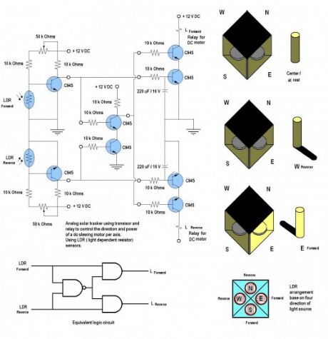
This is a simple and practical analog solar panel tracker circuit. Using four LDR (light dependent resistor) as a sensor in detecting the light source arranged as illustrated. When the light hit the LDR in a certain position, it will activate the circuit and trigger the relay to turn the slewing motor in the right direction until the sensor is fully shaded under its cover stopping the motor to its rest condition. (View)
View full Circuit Diagram | Comments | Reading(3490)
| Pages:57/2234 At 204142434445464748495051525354555657585960Under 20 |
Circuit Categories
power supply circuit
Amplifier Circuit
Basic Circuit
LED and Light Circuit
Sensor Circuit
Signal Processing
Electrical Equipment Circuit
Control Circuit
Remote Control Circuit
A/D-D/A Converter Circuit
Audio Circuit
Measuring and Test Circuit
Communication Circuit
Computer-Related Circuit
555 Circuit
Automotive Circuit
Repairing Circuit