
Circuit Diagram
Index 53
Automatic Street Light Circuits
Published:2013/11/14 19:34:00 Author:lynne | Keyword: Automatic Street Light Circuit

There have been lot of problems in street lights. Major problem in some places is every evening a person has to come and switch ON the street light and it should be again switched off in morning. Yes, this may not be the situation in everywhere but exists in many places.
So this problem can be overcome by using a simple circuit. Below shown circuit will be automatically switched ON and OFF during night and morning times respectively.
Automatic light schematic
In above circuit R1 can be used to adjust the sensitivity. And the working of the circuit is very simple. The LDR will have very low resistance during day time so the transistor Q1 will be in OFF condition. And during night time the resistance will be very high so automatically the transistor Q1 will be ON.
The Q1 is PNP transistor and the emitter of Q1 is given to base of Q2. So the Q2 transistor will be ON only if the transistor Q1 is ON. The TRIAC is used in the circuit to make is circuit complete. As the TRIAC will allow voltage to pass from either directions only when there is a certain threshold voltage in gate terminal. And the gate of TRIAC is controlled by transistor Q2.
So totally the lamp will be ON during night time and will be again switched off during day light. To change the sensitivity of the circuit to light adjust R2.
If you have any doubts, do not hesitate to comment below. We will come to you with an appropriate solution. (View)
View full Circuit Diagram | Comments | Reading(1954)
Simple Pulse Position Modulation Circuits
Published:2013/11/13 19:18:00 Author:lynne | Keyword: Simple Pulse Position Modulation Circuit

In pulse position modulation, the amplitude and width of the pulses are kept constant, while the position of each pulse with reference to position of reference pulse, is changed according to the instantaneous sampled value of the modulating signal. Below shown circuit diagram is the simplest pulse position modulation circuit using IC-555.With this type of circuit, the position of each pulse changes. Both width and period of the pulses vary with the modulating signal. Due to modulating signal at pin 5 ( Control voltage pin ), the UTP level changes to (2Vcc/3)+Vmod.
When Vmod increases, the UTP level increases and hence pulse width also increases. If Vmod decreases, UTP level decreases and pulse width also decreases. Thus the pulse width varies.
The pulse width is given by,
W = – (R1+R2) Cin [ (Vcc-UTP)/(Vcc-0.5UTP) ].
The period is given by,
T = W+0.693R2C
The space between the pulses which is constant is given by 0.693 R2C.This circuit has many application a quick example is, it is used in communication application for transferring voice or data.
(View)
View full Circuit Diagram | Comments | Reading(1095)
High Temperature Indicator Circuits
Published:2013/11/13 19:16:00 Author:lynne | Keyword: High Temperature Indicator

In some areas there is a need of temperature detectors which help them to detect temperature and indicate themwhether the temperature is low or not.
The components needed for the circuit are:
3 Resistors
1 Temperature dependent resistor
5v battery
Two 1n4007 diodes
One Op-Amp
One LED
And the circuit working is actually very simple, the Op-amp is connected as Non-inverting comparator. And a bridge circuit is made with the resistors and a Temperature Dependent Resistor. From above circuit R1, R2 and R3 are normal resistors but RT is Temperature Dependent Resistor.
The bridge resistance and RT are selected in such a way that as long as temperature is less than threshold value, the bridge is unbalanced by making Voltage at B more than voltage at A . Hence Vo = -Vsat and LED is reverse biased and remains OFF. When temperature becomes more than threshold then Voltage at B becomes less that Voltage at A hence it drives Vo = +Vsat. Due to this, LED glows and gives high temperature indication.
If you have any doubts about the above circuit, don’t hesitate to comment. (View)
View full Circuit Diagram | Comments | Reading(1053)
Single 1.2V NiMH Cell LEDs Flashlight Circuit
Published:2013/11/13 19:14:00 Author:lynne | Keyword: NiMH Cell LEDs Flashlight
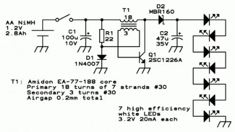
The single cell led flashlight circuit is a self-oscillating boost converter. A typical white LED has its best power-efficiency combination at about 20mA, and needs about 3.3V. This makes for a power of about 66mW per LED. In this circuit are 7 series LEDs so we need a driver circuit that will provide about 23V at 20mA, when fed from a 1.2V NiMH rechargeable cell or from a 1.5V alkaline cell.
When switching it on, R1 and D1 bias the transistor into the linear range, through the feedback winding on T1. That causes a current through the 18 turn winding, and thanks to the positive feedback the transistor is driven into saturation. At this moment there will be a base current defined like this: The 1.2V of the cell, plus the 0.2V induced in the feedback winding, minus the 0.7V base-emitter drop of the transistor, make a total of 0.7V, which applied to the 22 ohm resistor gives about 32mA base current. D1 is not conducting a significant current at this time, because the transistor clamps the base voltage to 0.7V and the 3 turn winding subtracts 0.2V from this, so that we end up with only 0.5V across the diode.
This base current keeps the transistor in saturation until its collector current reaches approximately 1A, while the transformer loads up. At this point the transistor will start getting out of saturation, which makes the feedback voltage drop. This very quickly puts the transistor into blockage. The collector voltage will soar as T1 forces current to keep flowing, until D2 starts conducting and discharges the transformer into C2, by means of a quite narrow pulse. During operation this pulse is about 24V high, so that the feedback winding develops -4V, which results in applying about -3.3V to Q1′s base, enough to switch it off very fast, but not enough to make the base reverse-conduct.
As soon as the transformer has fully discharged into C2, the voltage on it breaks down, and the transistor enters conduction to start a new cycle. The oscillating frequency is 30kHz, and the transformer operates at a peak flux density of 0.1 tesla, far away from saturation, and low enough to have very low loss. C2 has to eat the load pulses that start at about 1A, and has to keep the voltage constant enough to feed the LEDs an almost smooth DC. The value given works well. If anyone wants to build this circuit to run 24 hours a day for 30 years, it would be good to pick a capacitor rated for low ESR and a relatively high ripple current, but for flashlight use a plain standard 47µF, 35V electrolytic capacitor works great.
C1 is not strictly necessary. With a good NiMH cell, the circuit works the same without it, so you can save a few cents here. But with the capacitor in place, the circuit keeps working better when the cell is almost fully discharged and its internal resistance gets higher, so it’s better to include it. (View)
View full Circuit Diagram | Comments | Reading(1596)
How to Move a Trip Point of Op-Amp Comparator Circuits
Published:2013/11/12 20:02:00 Author:lynne | Keyword: Op-Amp Comparator
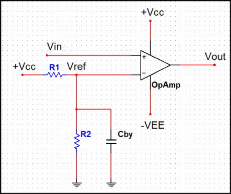

You all will befamiliar of basic comparator using a Op-Amp circuit. So today we will show you how to move a trip point of a Op-Amp comparator circuit. Maybe many of people already know this, but still this is the post forbeginners. So if you already know quit reading now only.
As shown in the above circuit, by application of a reference voltage to the inverting input rather than grounding it the trip can be moved. The reference voltage is given to the inverting input of a basic comparator using a potential divider consisting of resistors R1 and R2. The reference voltage Vref is derived using +Vcc and potential divider R1 and R2. Mathematically Vref is expressed as,
Vref = [+Vcc/(R1+R2)] R2
Now as long as the input voltage is less than Vref, the output is low i.e. -Vsat. When Vin becomes slightly greater than Vref, the Op-Amp output becomes high i.e. +Vsat. Thus the trip point is moved from Vin = 0 to Vin = Vref due to reference voltage applied to the inverting input terminal.
A bypass capacitor is used on the inverting input to reduce the amount of power supply ripple and noise appearing at the inverting input of Op-Amp. For effective bypassing of ripple and noise, the critical frequency of bypass circuit must be much lower than the ripple frequency of power supply.
The transfer characteristics of such a comparator is shown in above diagram which indicates positive trip point. Such a comparator is also called a limit detector as it detects the particular positive level of the input beyond which input goes high. The resistance R1 and R2 can be used to set the trip point anywhere between 0 and +Vcc.
The cut-off frequency of bypass circuit is,
fc = 1/[ 2π(R1||R2) Cby.
This must be much lower than the ripple frequency of the supply. (View)
View full Circuit Diagram | Comments | Reading(1576)
Basic Low Power AM transmitter Circuit
Published:2013/11/12 19:59:00 Author:lynne | Keyword: Basic Low Power AM transmitter
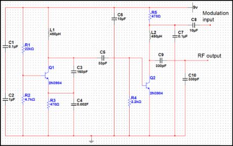
This transmitteris basic but allows transmission of audio to an AM radio. It consists of an RFoscillator operating in the AM broadcast band, together with a modulator stage,which mixes the incoming audio and the RF. A signal appears on the output, whichhas an AM component that can be picked up on a nearby AM radio receiver.
The transmitter consists ofoscillator stage Q1 and modulator/buffer stage Q2. Q1 is biased via R1, R2, and R3.L1, C3, and C4 form the tank circuit with feedback network C3-C4 providing feedbackto the emitter of Q1. RF voltage at the junction of C3 and L1 drives buffer/modulator stage Q2. Q2 is biased by base current produced by RF rectification in thebase emitter junction of Q2. C6 is an RF and AF bypass capacitor. C9, C10, and L2form the tank circuit for the collector of Q2. RF is taken from the junction of C9 andC10 and fed to ashort-wireantenna. Audio is fed to modulator Q2 via C8 and isolationresistor R5 and mixes with the RF signal in the collector circuit of Q2, producinga signal that has sum and difference frequencies if the RF carrier and AF input along with the carrier signal.
An AM signal appears atthe collector of Q2. Audio with an RMS voltage equal to about 0.7 times the collectorvoltage of Q2 is needed for full modulation of the output.Because of the high level of audio needed, the modulation obtained from this circuitis somewhat limited with conventional audio sources because several volts ofaudio into a few hundred ohms is needed. The circuit demonstrates the principle ofan AM transmitter, however, and with a suitable audio drive level, produces a well modulatedAM signal. (View)
View full Circuit Diagram | Comments | Reading(1170)
Sine to Rectangular Wave Conversion Circuits
Published:2013/11/12 19:55:00 Author:lynne | Keyword: Sine to Rectangular Wave Conversion Circuits
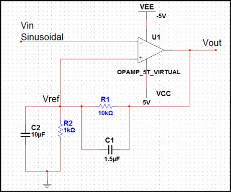
We have already given many posts on Op-Amp circuits. But the list of applications of Op-Amp will be keep on going. The best Op-Amp circuit which is used to convert sine waveform into rectangular waveform is the schmitt trigger circuit.
To avoid the false triggering, a positive feedback is used in a comparator circuit of an Op-Amp. Thus the comparator with positive feedback is called Schmitt trigger or regenerative comparator. The inverting schmitt trigger mode produces opposite polarity output. This isfed back to the non-inverting input which is of same polarity as that of output. This ensures positive feedback.
The above shown schematic is the sine to rectangular conversion circuit. For proper conversion of input signal from sine to rectangular, the input must be large enough to pass through both the tripping voltages.
Practically sometimes a capacitor C1 is connected in parallel with R1, as shown in the above schematic. The stray capacitance C2 forms the bypass circuit with R2. The use of speed-up capacitor C1 across R1 eliminates the effect of stray capacitance C2. Without speed-up capacitor, the stray capacitance C2 is required to be charged before the non-inverting input voltage changes. The speed-up capacitor used supplies the necessary charge to C2. For neutralizing the effect of stray capacitance, the minimum value of speed-up capacitor must be,
C1(min) = (R2/R1) C2.
When C1 is selected is greater than C1(min) then the switching of the output is very fast.
The frequency of the output of the Schmitt trigger is same as the frequency of the input signal.
The peak to peak value of the output rectangular waveform is approximately 2Vsat. (View)
View full Circuit Diagram | Comments | Reading(1033)
Rain Sound Generator-Sleep Aid in Case of Insomnia
Published:2013/11/11 19:23:00 Author:lynne | Keyword: Rain Sound Generator

Insomnia treatment consist mostly of sleeping pills consumption but this circuit is an alternative for that and consists of a simple circuitry that generates a rain sound effect. The japanese researches were the first to discover that sound of rain has a relaxing effect. With the help of this simple circuit we can generate the rain sound which can be a sleep aid in case of insomnia.T1 is used as a noise generator and its signal is amplified by the 741 IC and thru T2, R7 and C4 goes to a headset with low resistance. If you do not want to use the headphones then use a speaker with impedance between 4 and 16 Ω. With the help of P1 can adjust sound level and with P2 the tone.
Schematic of Rain Sound Generator Circuit
(View)
View full Circuit Diagram | Comments | Reading(2867)
Car Battery Charger with Transistors Circuit
Published:2013/11/11 19:20:00 Author:lynne | Keyword: Car Battery Charger

This car battery charger circuit can be used to charge 12V and 6V batteries. If it is used a transformer that can deliver 4A to 5A at a voltage between 12.6V and 16V then we can get rid of the switch for 6V or 12V batteries.
12V car battery charger circuit schematic
The car battery charging current is automatically limited to 4.2A. If there is a 600mV voltage on R1 (4A thru it), then the T1 transistor starts to conduct. Excessive charging current is avoided because the current value on T3′s base is limited. The difference between applied load current (at T4′s collector) and real voltage of the battery is balanced thru T4′s collector-emitter junction.
The power input of T4 (2N3055) is the product of load current and voltage difference already mentioned. When charging 6V car battery this power reaches a maximum of 40W. The rectifier diodes must be able to deliver 4A at 40V. T4 2N3055 must be mounted on a good heatsink in order to dissipate the heat. (View)
View full Circuit Diagram | Comments | Reading(1714)
Temperature Relay Circuits
Published:2013/11/11 19:18:00 Author:lynne | Keyword: Temperature Relay Circuit
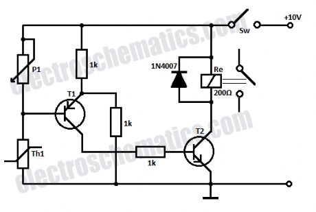
This simple temperature relay circuit can be used to signal a fire or setpoint for temperature monitoring function. You need to adjust P1 so that T1′s base voltage is 0.5V smaller than the emitter voltage at a temperature a little bit lower than the desired triggering (switching) temperature.If the temperature increases then T1 and T2 start conducting and the relay is closed (ON). If you want to use it as a cold relay or to signal an inferior temperature limit, then Th1 and P1 change places. After the relay is triggering you need to open switch S1 in order to stop the circuit. The nominal value of P1 must be choosed according to the used NTC thermistor and the switching temperature to be adjusted.
Temperature relay schematic
(View)
View full Circuit Diagram | Comments | Reading(1250)
12V SCR Battery Charger Circuits
Published:2013/11/10 20:09:00 Author:lynne | Keyword: SCR Battery Charger

This battery charger circuit differs from the norm in a number of ways, all of which make it difficult to understand. For this reason, I do not recommend it for the beginner.
Repairing /revamping a dead chargerWhat I started with was an inoperative 12amp battery charger. In hope of repairing it, I traced out the circuit, but did not like what I found—poor circuit design. So what I had to start with was an enclosure, ammeter, thermal overload interrupter, and center-tapped transformer all designed for battery charger application.
Since the maximum current delivered by the unit is a function of the transformer internal impedance, I recommend that the readers use the same type of transformer. If you are a good pack-rat (like me), you may already have a dead charger—or you can be on the lookout for one.
12V Battery Charger Schematic
SCR (Thyristor) RectifiersFirst of all, the two SCRs (silicon controlled rectifiers or thyristors) are connected with their anodes (stud or tab) grounded—this makes for excellent thermal transfer because no insulating hardware is required (if it is permissible to connect the negative terminal of the charger directly to the steel enclosure). If you do not wish to ground this point, use insulating hardware to electrically isolate the SCRs. This makes the transformer center-tap the positive terminal. The reason for this circuit placement is the ease of driving the SCR gates via the positive battery voltage—it is very unconventional as I have never seen this trick done before.
SCRs are the ideal power device choice for a battery charger because they can both regulate battery charging voltage and prevent fault current when the battery is inadvertently connected reverse. I have actually connected mine reverse and thought that the charger was inoperative until I realized what I had done.
Power Device SelectionI used two 2N690 stud-mount SCRs that I had available. Any in the series will work (2N683 through 2N690)—only the voltage rating differs and anything greater than 100V is good for the application. Other more inexpensive TO-220 candidates are: STMicroelectronics TYN616, Teccor/Littlefuse S6015L (isolated package), NXP 151-500C, or ON Seimconductor 2N6403G. Avoid sensitive gate devices.
Circuit CommonNormally circuits use a negative common—that is just the way the world seems to work, but in this case, it was more convenient to make the positive rail the common point and all visualization must be made with this in mind. The only exception is D7 that was installed to prevent damage should the battery get connected reverse. For visualization, simply short out D7. The conventional ground symbol is used for the negative rail. This tends to tie your brain in knots…
Voltage ReferenceA good battery charger tapers off when the battery voltage is above about 14V. For this to function, D6 is a 5.1V shunt zener regulator that puts out -5.1V relative to the positive rail. It is biased via R8.
Ramp GeneratorC1 and R4 form a ramp generator that generates a negative going sawtooth voltage (relative to the positive rail). It is reset to the positive rail via Q1 and Q2 at line voltage zero crossing. At zero crossing, there is no voltage at the anodes of D3 & D4 (relative to the positive rail), Q1 is off, Q2 is on and C1 is shorted. At all other points in the AC line cycle, C1 is charging. My line frequency is 60HZ. For 50HZ, increase the value of R4 to 82K.
Error AmplifierU1A is the error amplifier—it amplifies the difference between the -5.1V reference voltage and the feedback voltage at the arm of the V ADJ pot (R6). It is slowed down by the RC filter (R10 & C2), proportionately amplified by the ratio of R14 /R9, and integrated via C3. Perhaps you have heard of a PID (proportional, integral, derivative) control—this does just that, but neglects the derivative term as it is generally not required in most applications. If the error amplifier is not satisfied, it continues to integrate its output voltage until the feedback voltage equals the reference voltage. The function of the operational amplifier is to make the two input voltages equal.
The device selection here is the LF442 (or TL082) J-FET input operational amplifier. This is vital in this circuit because the common mode voltage range of the differential inputs must extend to the positive rail. Few op amps can do this (many have differential voltages that extend to the negative rail, but those will not work in this application).
Phase ComparatorU1B is the phase comparator. It compares the ramp voltage with the output of the error amplifier. It is also called the ramp-intercept technique. When the ramp generator voltage exceeds the error voltage signal (in the negative direction), the output of U1B switches negative and turns on Q3 thus providing gate current to the SCR that is forward biased. R13 is the gate current limiting resistor.
Flashing a Dead BatteryThe battery provides the power to begin operation of the regulator circuit, so if the battery is fully discharged it may be necessary to “flash” the battery terminals with a good battery to bootstrap the regulator into operation.I have toyed with the idea of installing a “Flash” pushbutton, but this adds more circuitry and I have not found it necessary. (View)
View full Circuit Diagram | Comments | Reading(2447)
1KHz Square Wave Generator Circuits
Published:2013/11/10 20:08:00 Author:lynne | Keyword: Square Wave Generator

You can build a simple 1KHz square wave generator using a few components and the LM3909 that is useful for testing audio equipment. It is powered from a single 1.5V battery cell and the maximum amplitude of the output signal is 1.1V. With P1 you can adjust the symmetry of the square wave signal and with P2 the amplitude.Square wave generator schematic
(View)
View full Circuit Diagram | Comments | Reading(1213)
12V SCR Battery Charger Circuit
Published:2013/11/10 20:06:00 Author:lynne | Keyword: SCR Battery Charger Circuit

You can build a simple 1KHz square wave generator using a few components and the LM3909 that is useful for testing audio equipment. It is powered from a single 1.5V battery cell and the maximum amplitude of the output signal is 1.1V. With P1 you can adjust the symmetry of the square wave signal and with P2 the amplitude.Square wave generator schematic
(View)
View full Circuit Diagram | Comments | Reading(1230)
Automatic Solar Garden Lights with LEDs Circuit
Published:2013/11/10 20:04:00 Author:lynne | Keyword: Automatic Solar Garden Light


Efficient automatic solar garder lights circuit with minimum components the best deal is that is completely auto and the Solar panel acts as a light detector. Switches the Lamp off at Dawn, charges the battery during daytime and switches the LED lights ON at dusk providing 100 Lumens illumination during the night.
The solar panel must provide 5.5V and 150mA. Assuming a 3.7V/1500mAh battery the charging will be complete in 8 hours at 200% capacity @ 180 mA. With 10 LEDs the power consumption would be 90 mA/hour providing a 10 hours illumination with light levels of 50 lumens to 60 lumens. With 20 LEDs the light intensity will be 100 to 120 lumens.
You can use any number of LEDs and battery capacity too. This would directly provide you the amount of illumination and time for illumination. If youusehighercapacitybatterythanthatrecommended thesolarpanelcurrentshouldbeincreasedproportionately. Current provided by solar panel should be 10% of battery capacity.
Solar garden lights circuit schematic
Bill of material for the solar garden lights
Resistor(1)4K7or5K6
Resistor(1)47Eor56Eoranyvalue(CurrentLimiting)
Transistor2N3906
Diode1N4001/7/1N4148(Any)
SolarPanel5.5v/200mA
Battery3.7v/1500mAh
SwitchSPST (View)
View full Circuit Diagram | Comments | Reading(1932)
220V Blinking LED Circuits
Published:2013/11/7 21:02:00 Author:lynne | Keyword: Blinking LED Circuit
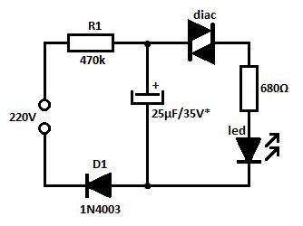
This is a simple blinking led circuit powered from 220V that can be used to mark special places or as voltage indicator. The voltage from the mains charges the capacitor through R1 resistor and D1 diode.As long as the capacitor’s voltage doesn’t exceeds the diac’s switching voltage the cap is acting as a blocked diode. After reaching the switching voltage the diac is conducting and the cap’s discharging current lights up the LED.
The blinking frequency of the LED depends mostly on the RC time constant (in this case T = 11 seconds). The capacitor’s voltage must be a little bit higher than the diac’s breakover voltage.
220 volts blinking LED schematic
With a 1N5758 diac the triggering voltage will be at 20V ± 2. (View)
View full Circuit Diagram | Comments | Reading(2230)
12V Battery Checker Circuits
Published:2013/11/7 21:00:00 Author:lynne | Keyword: Battery Checker Circuit

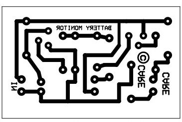
This is a 12V battery checker circuit that uses 3 LEDs that light up at their respective voltages. The red LED lights up when the battery voltage is between 8 to 10V, the orange one at voltages between 10.5V to 12V and the green one when the battery voltage is above 12.5V.This is a tried and tested battery checker circuit using one NPN and one PNP transistor. A PCB is given along with the schematic.
(View)
View full Circuit Diagram | Comments | Reading(2038)
12V Battery Level Indicator Circuits
Published:2013/11/7 20:55:00 Author:lynne | Keyword: Battery Level Indicator

This battery level indicator offers (5) LEDs that light up progressively as the voltage increases:
Red: Power Connected (0%)
Yellow: Greater than 10.5V (25%)
Green 1: Greater than 11.5V (50%)
Green 2: Greater than 12.5V (75%)
Green 3: Greater than 13.5V (100%)
Of course, you may select your own colors if desired.
12 Volts Battery Level Indicator Circuit Schematic
Operation of the battery level indicator
D1 is the voltage reference zener. Tied to this is a string of divider resistors (R2-6) that set the various fixed voltage levels. R7 & 8 form a voltage divider to that reduces the battery voltage by a factor of 3. U1 is an LM339 quad comparator that compares the various voltages from the two dividers. The comparator sections have open collector outputs that simply function as switches to operate the LEDs. D7 protects against reverse battery connection.
The LEDs are biased to operate at about 4mA which is quite bright if modern LEDs are used. This current can be adjusted simply by varying the series resistors (R9 through R13). The overall current drain as shown is about 25mA which tends to be wasteful for continuous operation. For energy conservation, connect to battery via a pushbutton (Push to Test).
Printed Circuit Board
I did a www.expresspcb.com SMT layout using 0805 size components, 1N753 zener and SOIC-14 IC. D7 is in a SOT-23 package. These components are about as small as I like to work with. The layout has not yet been carefully checked or built. Note that surprises abound when constructing prototypes.The circuit board measures only 0.5” x 1.5”. (View)
View full Circuit Diagram | Comments | Reading(1404)
Light Activated Switch Circuit
Published:2013/11/6 19:17:00 Author:lynne | Keyword: Light Activated Switch Circuit

The light activated switch circuit can be used for switching OFF a particular lamp or group of lamps in response to the varying ambient light levels.The unit once built can be used for switching OFF a lamp when dawn breaks and switching it ON when dusk sets in.The power supply is a standard transformer, bridge, capacitor network, which supplies a clean DC to the circuit for executing the proposed actions.
Automatic light activated switch circuit schematic
The LDR must be placed outside the box, meaning its sensing surface should be exposed toward the ambient area from where the light level is required to be sensed. The circuit can be used as an automatic street light controller system or a simple light activated switch. (View)
View full Circuit Diagram | Comments | Reading(1403)
Pathway Lighting with LEDs Circuit
Published:2013/11/6 19:15:00 Author:lynne | Keyword: Pathway Lighting

Simple pathway lighting that would provide illumination for the path at night. Extension for the Solar garden Light. The torroid is bifilar wound. The Torroid is 10mm and Cat 5 cable is wound around the same.Solar panels of 3.5 maybe difficult to procure using 2 2V panels in series could be used. If you do use 4V panel then suggest you add another diode in series with 1N4001 to drop voltage to contain voltage to the battery.
The characteristic voltage for a white LED is 3.2V but the addition of the torroid provides the boost to drive the white LED. If you cannot procure the battery as suggested you can use 600 mAH battery then do not go above 3/4 LED’s.
Pathway LED Lights Schematic
(View)
View full Circuit Diagram | Comments | Reading(1449)
Firefly Lights
Published:2013/11/6 19:07:00 Author:lynne | Keyword: Firefly Light
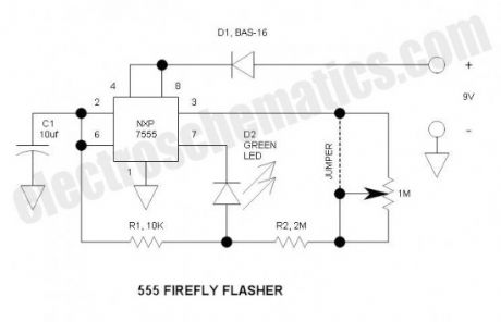
This firefly lights flasher is an easy, fun project. It can be built on the tiny circuit board, or on perf board.
Specifications
Battery life: approx 1 year using the NXP 7555 CMOS timer IC & standard alkaline battery, or about 6 months using the more common TI TLC555
Flash rate: approx 0.25 Hz (unless using optional potentiometer)
Dimensions: 14.5mm2
Minimum voltage: approx 6V
Schematic of the Firefly Flasher Circuit
Bill of Materials (if on perf board, use standard through-hole rather than SMT components)
PCB ExpressPCB.com
U1 NXP 7555 or TI TLC555 Timer IC, SOIC-8
R1 10K, 0805
R2 2M, 0805
R3 Potentiometer, 1M , 0.2” lead spacing (optional)
C1 10uF, 25V, X7R, Ceramic, 0805
D1 Diode, BAS16, or MMBD4148, SO23-3
D2 LED, Green, High Brightness, 0805
Battery Standard 9V
How the firefly lights works
It functions like almost any 555 astable timer, except that the LED is inserted into the capacitor reset path so that when pin 7 discharges C1 to common, this relatively high current must pass through the LED. In this way, the average battery current is only about 100µA. When battery voltage becomes very low, the LED threshold voltage prevents discharging C1 down to the lower threshold – when this happens, R2 finishes off the discharge because the output switches to ground potential the same time pin 7 turns on – you will find that this works on almost dead batteries that may be useless for other applications. D1 protects against accidental reverse battery voltage.
Background
Fireflies are common through Northeastern US and also in many other parts of the world. This green LED has the same color, flashes at about the same duration and has a similar repetition rate just like a real firefly (lightning bug). Put a number or these around your grounds and they will truly resemble fireflies – there will be no synchronization of the flashes. The only thing this cannot do is to fly – fireflies ascend as they flash, and they do not flash when perched to protect from predators. Also, this is much larger than the tiny firefly beetle that measures about 3 x 20mm.
(View)
View full Circuit Diagram | Comments | Reading(1271)
| Pages:53/2234 At 204142434445464748495051525354555657585960Under 20 |
Circuit Categories
power supply circuit
Amplifier Circuit
Basic Circuit
LED and Light Circuit
Sensor Circuit
Signal Processing
Electrical Equipment Circuit
Control Circuit
Remote Control Circuit
A/D-D/A Converter Circuit
Audio Circuit
Measuring and Test Circuit
Communication Circuit
Computer-Related Circuit
555 Circuit
Automotive Circuit
Repairing Circuit