
Circuit Diagram
Index 51
Christmas LED Lights Circuit
Published:2013/12/3 20:44:00 Author:lynne | Keyword: Christmas LED Lights Circuit

Using this simple Christmas LED lights decoration circuit, you can make an 18 LED flasher to decorate the Christmas Tree. The White, Blue and Red LEDs flash at different rates to give a colorful display. It is a light sensitive circuit so that it will turn on in the evening automatically and stays on till morning.
The circuit uses the popular Binary counter IC CD 4060 to flash the LEDs at different rates. Components C1, VR2 and R1 form the oscillator and the output pins 7, 5 and 4 become high / low sequentially. When one output turns high, a set of 3 LEDs turn on and when the same output turns off, the second set turns on. This sequence is similar in the other two sets of LEDs also but with different timings. The speed of the Flashing can be controlled through VR2.
Christmas LED Lights Decoration Circuit Schematic
LDR is provided with VR1 to activate the IC in the evening. In day light, LDR conducts and keep the reset pin 12 of IC1 high to inhibit it from working. When the day light ceases, pin12 becomes low and the flasher starts working. VR1 adjusts the sensitivity of LDR at the required light level. If more LEDs are required, increase the supply voltage to 18 volt DC. The circuit can be powered using a standard 12-18 volt 500 mA adapter.Use High bright transparent LEDs for attractive display. (View)
View full Circuit Diagram | Comments | Reading(2013)
LDR PC Desk Lamp
Published:2013/12/3 20:40:00 Author:lynne | Keyword: LDR PC Desk Lamp
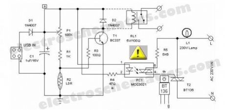

Most of the PC desk lamps available in the market light up whenever there is an input power. These don’t take into account whether there is a real need for the light or not. Here is an intelligent PC desk lamp circuit that overcome the problem.It senses the light level in the room to determine the actual need for light and lights up only if required. It is designed to work with the PC and remains on only when the PC in the table is in working state. It uses MOC3021.
Front end of the circuit is powered by the 5volt dc supply available from the usb port of the PC. When circuit is powered, the light sensor LDR (R2) resistance is low if there is sufficient light and thus most of the base current of transistor T1 finds an alternative easy path via LDR and T1 remains cutoff. While during dakness, the LDR behaves almost as an open circuit, and the current through sensitivity control preset pot (P1) and assosiated resistors (R1,R3) flows into the transistor’s base. As a consequence, T1 conducts to energise the opto-triac PC1. Next, the lamp driver triac T2 is fired through the opto-triac PC1 and switch on the power supply to the incandescent lamp.
The circuit can be constructed on a medium size PCB. After construction, enclose the finished circuit in a well insulated plastic cabinet. Then drill holes for mounting the ‘B’ type USB input socket, power switching termianls and the LDR etc. This circuit is meant for use in conjuction with Personal Computers to switch on an associated light sensitive table lamp/similar load. An optional electro magnetic relay can also be wired at the output of the circuit to switch heavy electrical load(s). For interconnection between PC and the control circuit, use a standard USB cable with an ‘A’ type connector on one end and a ‘B’ type connector at the other end.
LDR USB Desktop Lamp Circuit Schematic
(View)
View full Circuit Diagram | Comments | Reading(1104)
Light Alarm Circuit with LDR
Published:2013/12/2 21:09:00 Author:lynne | Keyword: Light Alarm Circuit

This musical light alarm circuit is very simple, uses only 7 components, a LDR and a 3.6 V battery or 3 x 1.2 volts rechargeable batteries. The well-known UM66 is used as the sound generator and will give a pleasent wake up alarm.
As you probably know the LDR is a light dependent resistor. Normally the resistance of an LDR is very high, sometimes as high as 1MΩ, but when they are illuminated with light resistance drops dramatically. In the circuit adjust the 220KΩ preset to the desired sensitivity, meaning adjusting the threshold point where the alarm start singing.
When there is light on the light dependent resistor the T1 transistor will start conducting and powers the UM66 musical integrated circuit. The produced musical note will be amplified by transistor T2 and fed into the 8Ω speaker.
On the UM66 IC are different numbers, each number giving a different musical note (in this example we use UM66T). You may use 2 x 1.5V batteries but 3 x 1.2V NiCad or NiMH are better because you can recharge them.
Light alarm electronic circuit schematic
(View)
View full Circuit Diagram | Comments | Reading(1173)
4011 IC Circuit
Published:2013/12/2 21:05:00 Author:lynne | Keyword: 4011 IC Circuit

The HEF4011B is a quad 2-input NAND gate. The outputs are fully buffered for the highest noise immunity and pattern insensitivity to output impedance. It operates over a recommended VDD power supply range of 3 V to 15 V referenced to VSS (usually ground). Unused inputs must be connected to VDD, VSS, or another input.The device is suitable for use over both the industrial (-40 oC to +85 oC) and automotive (-40 oC to +125 oC) temperature ranges. (View)
View full Circuit Diagram | Comments | Reading(1483)
IC CA3130 Circuit
Published:2013/12/2 21:03:00 Author:lynne | Keyword: IC CA3130 Circuit

CA3130A and CA3130 are op amps that combine the advantage of both CMOS and bipolar transistors. Gate-protected P-Channel MOSFET (PMOS) transistors are used in the input circuit to provide very-high-input impedance, very-low-input current, and exceptional speed performance. The use of PMOS transistors in the input stage results in common-mode input-voltage capability down to 0.5V below the negative-supply terminal, an important attribute in single-supply applications.The CA3130 Series circuits operate at supply voltages ranging from 5V to 16V, (±2.5V to ±8V). They can be phase compensated with a single external capacitor, and have terminals for adjustment of offset voltage for applications requiring offset-null capability. Terminal provisions are also made to permit strobing of the output stage. The CA3130A offers superior input characteristics over those of the CA3130.
(View)
View full Circuit Diagram | Comments | Reading(1144)
TL071, TL072, TL074 Circuit
Published:2013/12/1 20:34:00 Author:lynne | Keyword: TL071, TL072, TL074 Circuit

The JFET-input operational amplifiers in the TL07x series are similar to the TL08x series, with low input bias and offset currents and fast slew rate. The low harmonic distortion and low noise make the TL07x series ideally suited for high-fidelity and audio preamplifier applications. Each amplifier features JFET inputs (for high input impedance) coupled with bipolar output stages integrated on a single monolithic chip.TL071, TL072, TL074 Pinout
(View)
View full Circuit Diagram | Comments | Reading(1680)
Simple Square Wave Generator with 7400
Published:2013/12/1 20:28:00 Author:lynne | Keyword: Simple Square Wave Generator
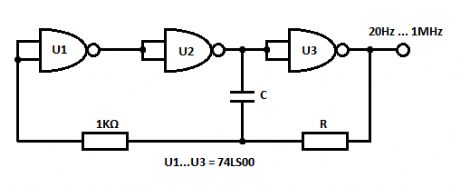
This is a very simple square wave generator circuit built with IC 74LS00 that can generate square signals with frequencies between 20 Hz and 1 MHz. Its stability is good enough for most applications. The output freq. is dimensioned through the RC components and time delay of the 3 inverter gates. The time delay of a logic gate is the elapsed time between a change of input state and the resulting change of the output state.To prevent the temperature and voltage supply from affecting the frequency of the square wave generator, the oscillator freq. fo must be smaller than 1/2tpn where:
tp = average delay time of each gaten = the number of gates
The above described oscillator has a tp of 10ns and n-3. The freq. is therefore:
fo << 1/2tpn = 1/2*10ns*3 = 16.6MHz
The voltage at the gate inputs varies from about _6V to -4V. The oscillation freq. can be made variable by using a 2.2KΩ potentiometer for R.
Square wave generator circuit schematic
(View)
View full Circuit Diagram | Comments | Reading(1068)
Simple Micro Ampere Meter Circuit
Published:2013/12/1 20:25:00 Author:lynne | Keyword: Simple Micro Ampere Meter Circuit
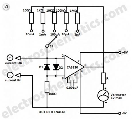
This simple micro ampere meter circuit can help in measuring small currents in five ranges: from 1 µA to 10 mA. The meter is working in this way: the current being measured Ix shifts the input voltage resulting to an output voltage with an inverted polarity.
The output voltage of the opamp CA3130 is proportional to the measured current Ix.By selecting the proper feedback resistors through S1, the output voltage by full meter deflection is 1 volt in all measuring ranges.
The value of the series resistor R must be selected for the particular meter being used. For example if a 1 mA meter is used, the total resistance (the sum of the resistor R and the coil resistance Ri of the meter) must be 1kΩ. If a 100 µA meter is used, the total resistance must be 100 kΩ. If needed, a potentiometer can be used for the R.
Micro ampere measurement circuit schematic
(View)
View full Circuit Diagram | Comments | Reading(1518)
Low Current Relay Circuit
Published:2013/11/28 21:02:00 Author:lynne | Keyword: Low Current Relay Circuit

This low current relay circuit is designed to be used in battery operated electronic devices. Its operating current is in micro amperes (µA). This is done by using a bistable relay and adding some components to force the relay to behave like a monostable relay.
A bistable relay stays at its last state when the power is turned off but consume at least 50mA trigger current. A monostable relay switches back to its original state when the power is turned off.
How does the low current relay works?
When the power is turned ON, the C1 charges via D1 and the relay coil and this current activates the relay. D1 ensures that the base of T1 is always more positive than its emitter and because of this T1 and T2 are always blocked.
Once the power is turned OFF, the emitter of T1 is coupled to the charge voltage at the positive pole of C1. Its base and the relay coil on the other hand are coupled to the negative pole of C1 and now T1 and T2 conduct, C1 can discharge through T2 and relay. The current flows to the relay coil but in reverse order so is activated to its other state.
It has the advantage of consuming little current, around 150 µA. For a reliable operation, select the relay’s operating voltage as 2/3 to 3/4 of the main power supply. For example is using a 12V power supply select a 9V relay.
Transistors replacements:T1 = 2SA499 = BC557, BC558T2 = 2SC734 = BC547, BC548
Low current relay switch circuit schematic
(View)
View full Circuit Diagram | Comments | Reading(1364)
Hi-Fi Stereo Preamp Circuit
Published:2013/11/28 20:56:00 Author:lynne | Keyword: Hi-Fi Stereo Preamp Circuit

This Hi Fi stereo preamplifier circuit is built with TDA1054 IC from SGS. TDA1054 is a 16-pin DIL package and integrates 2 separate preamp circuits.It is a low noise preamp with little or no problem in the building process.The first half of the circuit (IC1a) it has an input sensitivity of 3 mV and has a frequency correction composed of C5, C3, R6 and R8. The bass signal coming from phono input is amplified while the high signal is attenuated.
The selection of the input signal sources is done with switch S1. P1 and P2 are parte of a double potentiometer. They control the high tones and bass. There is no risk of overdrive in circuit due to the passive nature of the sound control.
P3 controls the volume of the signal fed to se second part of the circuit (IC1b) which functions as an operational amplifier.
P4 controls the balance between the left and right channels but in the schematic is shown only the preamp for one channel.Both channel have a gain of 24 at the middle setting of P4. If P4 is set to one extreme end, the gain difference between the 2 channels is about 12 dB.
HiFi stereo preamplifier schematic
(View)
View full Circuit Diagram | Comments | Reading(1630)
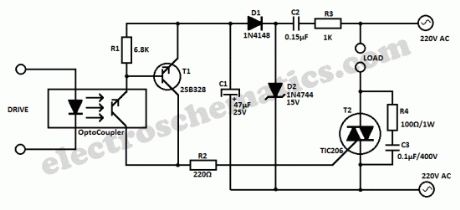
Universal Triac Control with Optocouplers
Published:2013/11/28 20:12:00 Author:lynne | Keyword: Universal Triac Control

This universal triac controller circuit with optocoupler solves the problem that triacs have when functioning at low temperatures (triac needs higher gate current) by adding a transistor at the output of the optocoupler circuit.The transistor amplifiers the trigger pulse coming from the optocoupler and the gate current is high enough to trigger the triac in all temperature cases.
How does the circuits works?
The base of the transistor is driven by the OC. C2 works as capacitive bias resistance to avoid power losses and it also helps avoid DC loading of the supply line. The switch current is limited by R3. D1 works as one-way rectifier while C1 works as ripple filter.D2 stabilize the rectified voltage to 15 V.
T1 conducts when the OC sends a pulse to its base. C discharges through the collector-emitter line. The trigger current is limited by R2 to around 40 mA.The discharge current time of C1 is less than 1 ms.
The RC circuit R4 and C3 protects the triac from voltage spikes.This is very important in all inductive loads.
Triac Optocoupler Controller Schematic
(View)
View full Circuit Diagram | Comments | Reading(2117)
LF355 Circuit
Published:2013/11/27 21:09:00 Author:lynne | Keyword: LF355 Circuit

LF355 circuits are monolithic J-FET input operational amplifiers incorporating well matched, high voltage J-FET on the same chip with standard bipolar transistors. This amplifiers feature low input bias and offset currents, low input offset voltage and input offset voltage drift, coupled with offset adjust which does not degrade drift or common-mode rejection.
The devices are also designed for high slew rate, wide bandwidth, extremely fast settling time, low voltage and current noise and a low 1/f noise level.
LF355 typical applications
precision high speed integrators
fast D/A and converters
high impedance buffers
wideband, low noise, low drift amplifiers
logarithimic amd photocell amplifiers
sample and hold circuits (View)
View full Circuit Diagram | Comments | Reading(2099)
Universal Triac Control with Optocoupler
Published:2013/11/27 21:07:00 Author:lynne | Keyword: Universal Triac Control with Optocoupler
This universal triac controller circuit with optocoupler solves the problem that triacs have when functioning at low temperatures (triac needs higher gate current) by adding a transistor at the output of the optocoupler circuit.The transistor amplifiers the trigger pulse coming from the optocoupler and the gate current is high enough to trigger the triac in all temperature cases.
google_ad_client= ca-pub-9265205501290597 ;google_ad_slot= 6648404198 ;google_ad_width=336;google_ad_height=280;
How does the circuits works?
The base of the transistor is driven by the OC. C2 works as capacitive bias resistance to avoid power losses and it also helps avoid DC loading of the supply line. The switch current is limited by R3. D1 works as one-way rectifier while C1 works as ripple filter.D2 stabilize the rectified voltage to 15 V.
T1 conducts when the OC sends a pulse to its base. C discharges through the collector-emitter line. The trigger current is limited by R2 to around 40 mA.The discharge current time of C1 is less than 1 ms.
The RC circuit R4 and C3 protects the triac from voltage spikes.This is very important in all inductive loads.
Triac Optocoupler Controller Schematic