
Signal Processing
Index 109
Optically_isolated_power_transistor
Published:2009/7/22 22:26:00 Author:Jessie
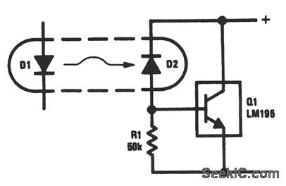
In this circuit, D1 and D2 can be part of almost any standard optocoupler or optoisolator. With no drive, R1 absorbs the base current of Q1, holding Q1 off. When power is applied to D1 (or to the LED of an optocoupler), D2 allows current to flow from the collector to base. Less than 20 μA is required from D2 to turn the LM1195 fully on。 (View)
View full Circuit Diagram | Comments | Reading(598)
TRANSISTOR_TESTER_WITH_SPEAKER
Published:2009/7/22 22:53:00 Author:Jessie

Blocking-oscillator test circuit provides tone from speaker only when transistor is good (not open, shorted, or leaky). Runaway transistors con be detected by providing npn-pnp switch and reversing it to stop oscillation for a few seconds, then restoring correct position. If transistor then oscillates al different frequency or will not resume oscillation, it is a runaway.-L. G. Sands, Dynamic Testers For Transistors, Electronics, 33:8, p 66-67. (View)
View full Circuit Diagram | Comments | Reading(697)
DYNAMIC_TRANSISTOR_TESTER
Published:2009/7/22 22:51:00 Author:Jessie

Uses blocking oscillator and depends on fact that open, shorted, or excessively leaky transistors will not oscillate. Good transistors should oscillate with R1 set at zero, and make neon lamp glow if S1 is on.-L. G. Sands, Dynamic rosters For Transistors, Electronics, 33:8, p 66-67. (View)
View full Circuit Diagram | Comments | Reading(1115)
LASCR_CONTROLLED_OSCILLATOR
Published:2009/7/6 6:15:00 Author:May
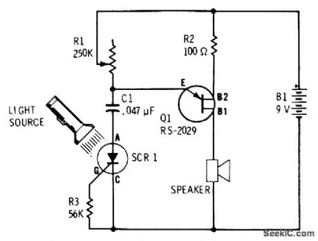
UJT relaxation oscillator having loudspeaker load produces single click each time flash of light falls on light-activated SCR Setting of R1 determines whether circuit produces series of pulses or tone burst during time light is on Oscillator frequency Increases with light intensity.-F. M. Mims, Semiconductor Proiects, Vol.2, RadioShack, Fort Worth, TX, 1976, p 71-77. (View)
View full Circuit Diagram | Comments | Reading(1586)
SOLAR_POWER_OSCILLATOR
Published:2009/7/6 6:14:00 Author:May
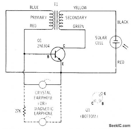
Supply voltage for single-transistor audio oscillator is generated by Radio Shack 276-115 selenium solar cell that produces about 0.35 V in bright sunlight. With cell 3 feet away from 75-W incandescent lamp, oscillator frequency is about 2400 Hz. Frequency drops as light increases. Transformer is 273-1378.-F. M. Mims, Transistor Projects, Vol. 2, Radio Shack, Fort Worth, TX, 1974, p 53-58. (View)
View full Circuit Diagram | Comments | Reading(965)
5_kHz_PHOTOCELL_OSCILLATOR
Published:2009/7/6 6:04:00 Author:May
Provides 5-V pulses at about 5 kHz only if photocell is illuminated by its companion LED. Repetition rate varies with illumination, so interruption or attenuation of light produces easily detected frequency change that can be used as control signal. Applications include fail-safe interruption monitor and illumination transducer. Oscillation stops if beam is completely interrupted or if strong ambient light falls on photocell.-H. L. Hardy, FM Pulsed Photocell Is Foolproof, EDN Magazine, March 5, 1975, p 72. (View)
View full Circuit Diagram | Comments | Reading(706)
SOUND_EFFECTS_GENERATOR_1
Published:2009/7/6 6:03:00 Author:May

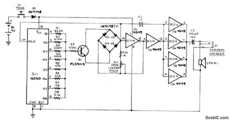
This circuit can generate a European police-car slren,bird nolses,spaceship sounds,etc.In addition,it can be put to use as a doorbell,an alarrm,etc.The circuit consists of four parts:a binary counter,a D/A converter,a VCO,and an audio output amplifier.The initial frequency of oscillation IS determined by potentiometer R11.The VCO firstoscillates at a relatively low frequency,and gradually picks up speed as the control voltage supplied by the D/A converter mcreases.The D/A converter IS the group of resistorsR1-R8.When none of IC1's outputs IS active,little current will flow into the base of Q1,so the VCO's control voltage will be low.As more and more counter outputs becomeactive,base current mcreases,and thereby so does the VCO's frequency of oscillation.The VCO itself IS composed of IC2-a,IC2-b,Q1,and the timing network comprising D1-D4,C1,R10,and R11.The buffer amplifier is made up of the four remammg gatesfrom IC2,all wired In parallel.
(View)
View full Circuit Diagram | Comments | Reading(1338)
INVERSE_RIAA_RESPONSE_GENERATOR
Published:2009/7/6 5:49:00 Author:May
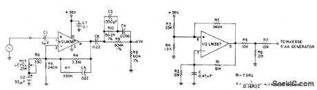
Used in design, construction, and testing of phonograph preamp. Provides opposite of play-back characteristic, Passive filter is added to output of National LM387, used as flat-response adjustable-gain block. Gain range is 24 to 60 dB, set in accordance with 0-dB reference gain (1 kHz) of preamp under test. Input is from 1-kHz square-wave generator, which can be built with other half of LM387 connected as also shown.-D.Bohn, Invese RIAA/Square Wave Generator, Audio, Feb. 1977, p 65-66. (View)
View full Circuit Diagram | Comments | Reading(1453)
YELP_OSCILLATOR
Published:2009/7/6 5:44:00 Author:May


Close the pushbutton switch and the circuit starts the siren up-shifting to a higher frequency. Release it and the tone slides down until S2 is closed again. Tone quality is adjusted by changing the 0.022 μF capacitor.
(View)
View full Circuit Diagram | Comments | Reading(739)
60_Hz_CLOCK_PULSE_GENERATOR
Published:2009/7/6 5:42:00 Author:May

The circuit provides a clean, stable square wave and it will operate on anywhere from 6 to 15 volts. The IC and color-burst crystal are the kind used in TV receivers. The 3.58 MHz output makes a handy marker signal for shortwave bands. (View)
View full Circuit Diagram | Comments | Reading(890)
20_KC_TRIGGER_GENERATOR
Published:2009/7/23 21:09:00 Author:Jessie
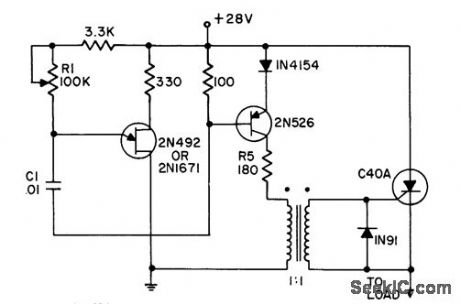
Uses ujt to drive 2N526 transistor from cutoff to saturation. Since energy in C1 is not used to trigger ser, small capacitor can be used, thereby increasing operating frequency limit.- Transistor Manual, Seventh Edition, General Electric Co., 1964, p 333. (View)
View full Circuit Diagram | Comments | Reading(646)
WARBLING_TONE_GENERATOR
Published:2009/7/6 5:31:00 Author:May

The circuit use two unijunction transistors. The low-frequency sawtooth generated by Q1 modulates the high-frequency tone generated by Q2. The output should feed into a high-impedance amplifier. Q1 = Q2 = 2N4871.
(View)
View full Circuit Diagram | Comments | Reading(929)
WARBLE_GENERATOR
Published:2009/7/6 5:25:00 Author:May

The circuit uses a pair of 555 timers or a single dual timer. Capacitor C1 controls the speed of the warble, while C2 determines the pitch. The values shown should produce quite a distinctive signal. (View)
View full Circuit Diagram | Comments | Reading(654)
5_MHz_VFO
Published:2009/7/6 5:23:00 Author:May
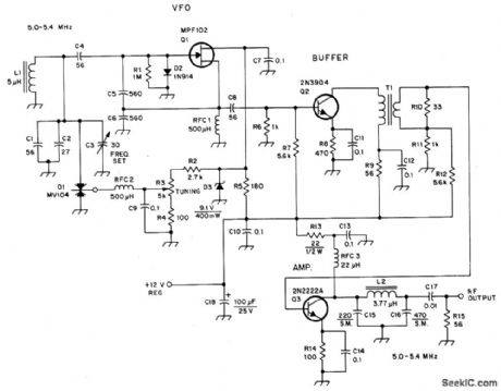
Circuit Notes
AJFET (Q1) serves as the oscillator. D2 helps to stabilize the transistor by limiting positive sinewave peaks and stabilizing the bias. Output from Q1 is supplied to a class A buffer, Q2. It operates as a broadband amplifter by means of T1, which is untuned. Output amplifter Q3 is also a class A stage. A low-pass, single-section ftlter is used at the output of Q3 to remove some of the harmonic currents generated within the system.The ftlter output impedance is 50 ohms. The injection level to the mixer is 600 mV p-p. (View)
View full Circuit Diagram | Comments | Reading(1085)
TONE_BURST_GENERATOR
Published:2009/7/6 5:05:00 Author:May
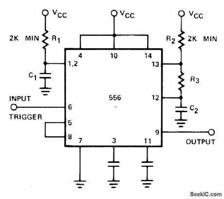
The dual timer makes an excellent tone burst generator. The first half is connected as a one shot and the second half as an oscillator.
The pulse established by the one shot turns on the oscillator allowing a burst of pulses to be generated. (View)
View full Circuit Diagram | Comments | Reading(0)
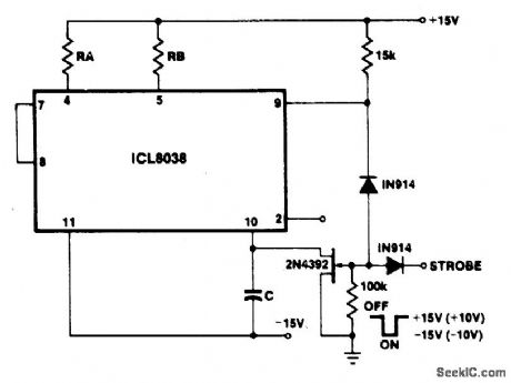
STROBE_TONE_BURST_GENERATOR
Published:2009/7/6 5:02:00 Author:May
View full Circuit Diagram | Comments | Reading(1265)
SQUARE_WAVEFORM_MULTIBURST_GENERATOR
Published:2009/7/6 4:55:00 Author:May

The generator described here IS intended for multiburst signal square waveformgeneration and can be used as a device for characterizing the response of TV monitoramplifiers as shown.The circuit is an RC oscillator with NAND gates(IC4-4011),withits capacitor C changed periodically by means of bilateral switches(IC2,IC3-4016),Thecontrol inputs of bilateral switches are driven by the outputs of a counter/decoder(IC1-4017)the operation of which is determined by generated clock pulses,SO that theyoccur eight times at half-picture (field).These pulses are locked to vertical blank pulses. Horizontal synchronizatiOn is achieved by means of composite blanking pulses (negative polarization) applied to pms 1 and 5 of IC4,The oscillator frequency changesh the following(liscrete steps:460 kHz,680 kHz,900 kHz,1400 kHz,2700 kHz,3600kHz,for the time of one frame。The video signal is fed on a mlxer where it is superimposedwith a composite sync signal. (View)
View full Circuit Diagram | Comments | Reading(976)
SINGLE_TONE_BURST_GENERATOR
Published:2009/7/6 4:53:00 Author:May

The tone burst generator supplies a tone for one-half second after the power supply is activated; its intended use is a communications network alert signal. Cessation of the tone is accomplished at the SCR, which shunts the timing capacitor C1 charge current when activated. The SCR is gated on when C2 charges up to the gate voltage which occurs in 0.5 seconds. Since only 70 μA are available for triggering, the SCR must be sensitive enough to trigger at this level. The triggering current can be increased, of course, by reducing R2 (and increasing C2 to keep the same time constant). If the tone duration must be constant under widely varying supply voltage conditions, the optional Zener diode regulator circuit can be added, along with the new value for R2 R2' = 82 kΩ. If the SCR is replaced by an can transistor, the tone can be switched on and off at will at the transistor base terminal. (View)
View full Circuit Diagram | Comments | Reading(830)
TRANSFORMERLESS_BASE_MODULATOR
Published:2009/7/23 20:09:00 Author:Jessie
Requires only one audio transistor, and readily provides 100% modulation. Modulated output power is 660 mw for CB transmitter. Audio quality is excellent.-B. Rheinfelder, Modulation Techniques for Transistorized A.M Transmitters, FEE, 11:7, p 54-57. (View)
View full Circuit Diagram | Comments | Reading(1017)
20_20000Hz_SINE_SQUARE
Published:2009/7/6 4:35:00 Author:May

Opamp is used as tuned circuit driven by square wave from yoltage comparator Frequeny is controlled by R1-R3, C1, and C2, with R3 providing tuning.Comparator is fed with resulting sine wave to obtain square wave for feedback to input of tuned circuit, to cause oscillation. Zener stabifizes amplitude of square wave that is fed back.R6 and C5 provide DC negative feedback around comρarator to ensure starting.Values of C1 and C2 are equal,and range from 0.4 μF for 18-80Hz to 0.002 μF for 4.4-20 kHz.-''Easily Tuned Sine Wave Oscillator,″National Semiconducotor,Santa Clara,CA,1971,LB-16. (View)
View full Circuit Diagram | Comments | Reading(944)
| Pages:109/195 At 20101102103104105106107108109110111112113114115116117118119120Under 20 |
Circuit Categories
power supply circuit
Amplifier Circuit
Basic Circuit
LED and Light Circuit
Sensor Circuit
Signal Processing
Electrical Equipment Circuit
Control Circuit
Remote Control Circuit
A/D-D/A Converter Circuit
Audio Circuit
Measuring and Test Circuit
Communication Circuit
Computer-Related Circuit
555 Circuit
Automotive Circuit
Repairing Circuit