
Signal Processing
Index 102
PHASE_SHIFT_KEYER
Published:2009/7/21 7:49:00 Author:Jessie

Used with double-side-band suppressed-carrier modulation. Crystal-controlled Colpitts oscillator drives transistor gate, which in turn feeds conventional tuned pentode r-f amplifier and tuned cathode follower.-J. Dysinger, W. Wyland, and It Wood, New Suppressed-Carrier Modulation Technique, Electronics, 33:6, p 47-49. (View)
View full Circuit Diagram | Comments | Reading(931)
2185_MC_MARINE_BAND_TRANSMITTER
Published:2009/7/21 7:48:00 Author:Jessie
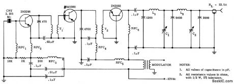
Grounded-base Colpitts oscillator uses series-mode crystal with driver and output stage. Current drain is only 1.5 amp from storage battery. No converter is required. Output is 13-w rms carrier.-R. J. Brubaker, An All. Solid-State Marine Band Transmitter, Motorola Application Note AN-156, Feb. 1966. (View)
View full Circuit Diagram | Comments | Reading(638)
STEPPED_FREQUENCY_EXCITER
Published:2009/7/21 7:47:00 Author:Jessie
Provides crystal-controlled output frequency in 100-kc steps at 1-sec intervals from 31.05 to 54.95 Mc, with each step an odd multiple of 50 kc. Used to control pulse transmitter and receiver at widely separated locations, for observation of mutual propagation conditions between the two points. Frequency control of r-f oscillator is obtained by mixing sample r-f signal with 1-Mc reference and comparing components of product with 50-kc pulse spectrum supplied by pulse generator V6B.-Frequency Stepper for Radio Propagation Tests, Electronics, 32:4, p 44-46. (View)
View full Circuit Diagram | Comments | Reading(622)
DUAL_PULSE_TRIGGER
Published:2009/7/21 7:57:00 Author:Jessie
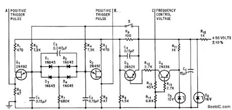
Dual triggers supply alternating pulses for driving d-c to d-c voltage converter connected to A and B. Frequency of triggering can be adjusted from 650 to 900 cps by varying base-to-base voltages of unijunction transistors.-T. Wilson, Voltage Controls Dual-Pulse SCR Trigger, Electronics, 37:28, p 62-63. (View)
View full Circuit Diagram | Comments | Reading(621)
INPUT_TURNS_BOTH_TRANSISTORS_ON
Published:2009/7/21 7:55:00 Author:Jessie
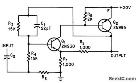
Unlike Schmitt trigger, both transistors stop conduction when input is removed.-L. L. Kleinberg, Complementary Shaper Replaces Schmitt Trigger, Electronics, 37:26, p 66. (View)
View full Circuit Diagram | Comments | Reading(670)
NARROWBAND_162_180_MC_TRANSMIITER
Published:2009/7/21 7:53:00 Author:Jessie

First stage acts as buffer for oscillator, while Q2 and Q3 multiply frequency. Class-C power amplifier using two SM2498 transistors in parallel delivers 300 mw to 50-ohm load.-Texas Instruments Inc., Solid-State Communications, McGraw-Hill, N.Y.,1966, p 325. (View)
View full Circuit Diagram | Comments | Reading(546)
735_MC_SELF_MODULATED_CRYSTAL
Published:2009/7/21 7:52:00 Author:Jessie
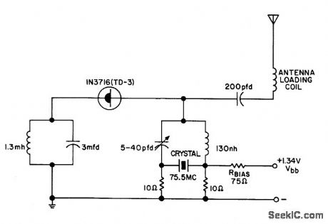
Uses tunnel diode oscillator to modulate crystal. Transistor Manual, Seventh Edition, General Electric Co., 1964, p 357. (View)
View full Circuit Diagram | Comments | Reading(817)
Color_TV_subcarrier_generator
Published:2009/7/21 8:06:00 Author:Jessie
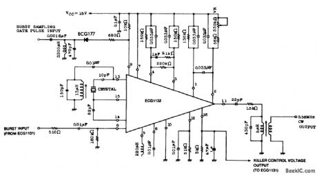
Color TV subcarrier generator. The crystal shown is for 3.58 MHz. The ECG1131 noted on the schematic is a chroma signal amplifier. The ECG1132 is a 16-pin DIP (courtesy GTE Sylvania Incorporated). (View)
View full Circuit Diagram | Comments | Reading(567)
50_MHZ_VHF_CRYSTAL_OSCILLATOR
Published:2009/7/7 7:57:00 Author:May

Figure 21-14 shows a 50-MHz oscillator operating on a third harmonic. The collector's load resistor R1 has been increased because the quartz crystal's internal series resistance RS increases with frequency in the VHF range. The crystal's internal series resistance RS is 3Ω , and the transistor's minimum current gain HFE is 100. Using the same technique as for the 20 MHz oscillator, the external series RLCL equivalent load seen by the 50 MHz crystal is 5.6Ω (RL) and 1000 pF (CL). (View)
View full Circuit Diagram | Comments | Reading(940)
100_MHz_VHF_CRYSTAL_OSCILLATOR
Published:2009/7/7 7:53:00 Author:May

Figure 21-13 shows a 100-MHz oscillator operating on the fifth harmonic. Again to maintain the transistor's gain, note the increase in the collector's load resistance R1 because of the increase in the quartz crystal's internal series resistance Rs. C3 is needed at frequencies above 50 MHz to tune out the shunting effect of L1 on R1, to maintain a high load resistance for the transistor and get enough gain for oscillation.The equivalent series RLCL load across the crystal is 8.2 Ω (RL) and 200 pF (CL).
(View)
View full Circuit Diagram | Comments | Reading(1819)
MARKER_GENERATOR
Published:2009/7/7 7:50:00 Author:May
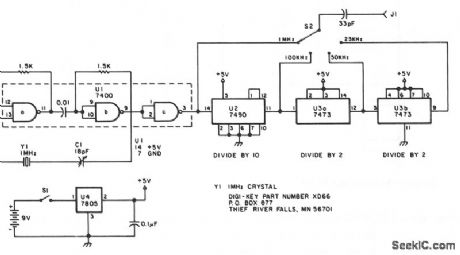
The oscillator section uses three sections of a 7400 quad NAND gate integrated circuit. The 1-MHz signal from the oscillator is fed into a 7490 decade counter configured to divide by ten, providing the 100-kHz signal. To obtain the 50 and 25 kHz outputs, the 100-kHz signal is further divided by 7473 dual J-K flip-flop. The first half of the 7473 divides the 100-kHz signal by two, yielding the 50 kHz signal. The second half of the 7473 again divides by two, giving the 25 kHz signal. S2 selects the output, a square wave, rich in harmonics. The generator can be powered from any convenient 6 to 12 Vdc source. A 7805 ftxed-voltage regulator supplies the regulated voltage for the oscillator and the divider chips. The generator described here is powered by a 9-V transistor radio battery. (View)
View full Circuit Diagram | Comments | Reading(2044)
20_MHz_VHF_CRYSTAL_OSCILLATOR
Published:2009/7/7 7:47:00 Author:May

A typical circuit at 20 MHz is shown. The crystal, which has an internal series resistance RS, of 14 Ω , oscillates at its third harmonic. The diode clamp D1 and D2 provides a constant amplitude control. The transistor operates continuously in a linear mode over a complete cycle of oscillation, and reflects a reasonably constant load across the crystal at an times. (View)
View full Circuit Diagram | Comments | Reading(694)
TEMPERATURE_COMPENSATED_CRYSTAL_OSCILLATOR
Published:2009/7/7 7:27:00 Author:May

This circuit uses LTC1043 to differentiate between a temperature sensing network and a dc reference. The single-ended output biases a varactor-tuned crystal oscillator to compensate drift. The varactor crystal network has high dc impedance, eliminating the need for an LTC1043 output amplifier.
(View)
View full Circuit Diagram | Comments | Reading(0)
CRYSTAL_CONTROLLED_REFLECTION_OSCILLATOR
Published:2009/7/7 7:25:00 Author:May


This unit is easily tunable and stable, consumes little power, and costs less than other types of oscillators that operate at the same frequencies. This unusual combination of features is made possible by a design concept that includes operation of the transistor well beyond the 3 dB frequency of its current-versus-frequency curve. The concept takes advantage of newly available crystals that resonate at frequencies up to about 1 GHz.
The emitter of transistor Q is connected with variable capacitor C1 and series-resonant crystal X.The emitter is also connected to ground through bias resistor R1. The base is connected to the parallel combination of inductor L and capacitor C3 through dc-blocking capacitor and C4 and is forward biased with respect to the emitter by resistors R3 and R4. Impedance Z could be the 220-Ω resistor shown or any small impedance that enables the extraction of the output signal through coupling capacitor C2. If Z is a tuned circuit, it is tuned to the frequency of the crystal. (View)
View full Circuit Diagram | Comments | Reading(748)
TWO_GATE_QUARTZ_OSCILLATOR
Published:2009/7/7 7:18:00 Author:May

A SN7400 quartz crystal and a resistor provide a square-wave output of approximately 3.5 V. The circuit operates reliably at frequencies from 120 kHz to 4 MHz. (View)
View full Circuit Diagram | Comments | Reading(2315)
VOLTAGE_CONTROLLED_CRYSTAL_OSCILLATOR
Published:2009/7/7 7:16:00 Author:May

A voltage-variable capacitance tuning diode is placed in series with the crystal feedback path. Changing the voltage on VR varies the tuning diode capacitance and tunes the oscillator. The 510-KΩ resistor, R1, establishes a reference voltage for VR-ground is used'm this example. A 100-KΩ resistor, R2, isolates the tuning voltage from the feedback loop and 0.1-μF capacitor C2 provides ac coupling to the tuning diode. The circuit operates over a tuning range of 0 to 25 V. It is possible to change the tuning range from 0 to 25 V by reversing the tuning diode Dl. Center frequency is set with the 2 -60 pf trimmer capacitor.Deviation on either side of center is a function of the crystal frequency. The table in Fig. 21-7 shows mea-sured deviation in parts per million for several tested crystals. (View)
View full Circuit Diagram | Comments | Reading(1488)
LOW_FREQUENCY_PIERCE_OSCILLATOR
Published:2009/7/7 7:14:00 Author:May

The Pierce circuit oscillates at 4 kHz.At low frequencies,the crystal's internal senes resistance RS isquite high (45 K at 4 kHz).Therefore,all FET-based source follower is included to prevent Q1 from loading the crystal output. (View)
View full Circuit Diagram | Comments | Reading(840)
SIMPLE_CMOS_CRYSTAL_OSCILLATOR
Published:2009/7/7 7:10:00 Author:May

The circuit is an inverter set up as a linear amplifier. Adding the crystal and capacitors to the feedback path, we tum the amplifier into an oscillator and force it to oscillate at, or least very near, the crystal's resonant frequency. Trimmer capacitor C2 adjusts the actual operating frequency of the circuit. The crystal should be a parallel-resonant type; maximum frequency will depend partly on supply voltage, but it should be possible to go to at least 1 MHz. (View)
View full Circuit Diagram | Comments | Reading(2053)
1_MHz_PIERCE_OSCILLATORS
Published:2009/7/7 7:09:00 Author:May

Simple network design is a key feature of the Pierce circuit, as these 1-MHz oscillators illustrate .Operating the crystal slightly above resonance (Fig.21-5a) requires only one high-gain transistor stage.Operating it exactly at series resonance (Fig. 21-5b) requires an extra RC phase lag and two transistors which can have lower gain. (View)
View full Circuit Diagram | Comments | Reading(2333)
EASY_START_UP_CRYSTAL_OSCILLATOR
Published:2009/7/7 7:06:00 Author:May


This low cost, crystal-controlled oscillator uses one TTL gate. Two factors ensure oscillator start-up: The connection of NAND gates G1, G2, and G3 into an unstable logic configuration and the high loop gain of the three inverters. Values of R1, R2, C1, and C2 aren't critical; select them so the oscillator operates at a frequency 70 to 90% higher than the crystal frequency when the crystal is disconnected. For 1-2 MHz operation, a low-power 54L00IC is recommended; for a 2-6 MHz, a standard 5400 type; and for 6-20 MHz, a 54H00 or 54S00.
(View)
View full Circuit Diagram | Comments | Reading(802)
| Pages:102/195 At 20101102103104105106107108109110111112113114115116117118119120Under 20 |
Circuit Categories
power supply circuit
Amplifier Circuit
Basic Circuit
LED and Light Circuit
Sensor Circuit
Signal Processing
Electrical Equipment Circuit
Control Circuit
Remote Control Circuit
A/D-D/A Converter Circuit
Audio Circuit
Measuring and Test Circuit
Communication Circuit
Computer-Related Circuit
555 Circuit
Automotive Circuit
Repairing Circuit