
Signal Processing
Index 110
SINE_COSINE
Published:2009/7/6 3:58:00 Author:May

Uses National SK0003 sine/cosine look-up table kit consisting of four MOS ROMs and three output adders. Combination implements equation sin θ=sin M cos L + cos M sin L.Worst-case error is 1 5/8 bits in least significant bit. Cosine is approximated with loss in resolution of1/2 bit in 11-bit input or1/4 bit in 10-bit input.- Memory Databook, National Semiconductor, Santa Clara, CA, 1977, p 6-98-6-99. (View)
View full Circuit Diagram | Comments | Reading(848)
LOW-DRAIN_2_MHz_FRONT_END
Published:2009/7/6 2:49:00 Author:May
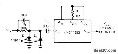
Simple CMOS linear front end for 5-MHz battery-operated counterreduces power drain and makes it proportional to input frequency,With no input,drain is only a few microamperes Half of COUNTER MC14583 CMOS Schmitt trigger forms front end operating from single 6-V battery used In counter,Upper frequency limit is about 3 MHz,and input sensitivity is 400 mV.-D Aldridge,CMOS Counter Circuitry,Slashes Battery Power Requirements,EDN Magazine,Oct,20,1974,p 65-71.
(View)
View full Circuit Diagram | Comments | Reading(923)
WAVEFORM_GENERATOR
Published:2009/7/6 2:48:00 Author:May
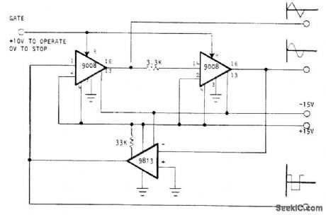
Two Optical Electronics 9008 integrators and 9813 comparator together generate choice of sine, square, and triangle waveforms suitable for system testing and display generation. Square wave is typically± 13.5 V with 20-μs transition time. Trianglewave is ±10V with better than 0.1% triangle linearity. Comparator senses zero crossings of sine-wave output to produce square waves, thus completing feedback loop. Integrators are commanded at pin 8 for zero output, so triangle and sine outputs can be made to start from zero.-''Waveform Generator, Optical Electronics, Tucson, AZ, Application Tip 10257. (View)
View full Circuit Diagram | Comments | Reading(0)
100_MHz_CRYSTAL_OSCILLATOR
Published:2009/7/6 2:44:00 Author:May
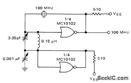
Developed for frequency counter that uses standard ECL components. Crystal can be changed to 10 MHz when measuring TTL performance.-W. B.Blood, Jr., Measure Frequency and Propagation Delay whh High Speed MECL Circuits, Motorola, Phoenix, AZ, 1972, AN-586 p 3.
(View)
View full Circuit Diagram | Comments | Reading(89)
3_TRANSISTOR_UHF_TUNER
Published:2009/7/23 21:40:00 Author:Jessie

Conversion gain is up to 9 db and noise figure around 8 db, with drain of 18 ma at 12 v.-Transistors Provide Gain in TV Tuner, Electronics, 35:26,p 25. (View)
View full Circuit Diagram | Comments | Reading(1215)
VOLTAGE_CONTROLLED_RAMP_GENERATOR
Published:2009/7/6 2:03:00 Author:May

Circuit NotesThe current source formed by Q1 in conjunction with capacitor C1 set the duration time of the ramp. As the positive dc voltage at the gate is changed, the peak point firing voltage of the PUT is changed, which changes the duration time, i.e., increasing the supply voltage increases the peak point firing voltage causing the duration time to increase. (View)
View full Circuit Diagram | Comments | Reading(791)
RAMP_GENERATOR
Published:2009/7/6 2:01:00 Author:May
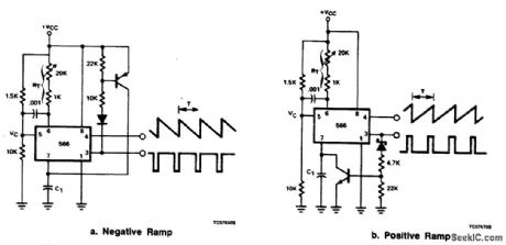
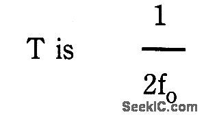

Circuit Notes
The 566 can be wired as a positive or negative ramp generator. In the positive ramp generator, the external transistor driven by the Pin 3 output rapidly discharges C1 at the end of the charging period so that charging can resume instantaneously. The pnp transistor of the negative ramp generator likewise rapidly charges the timing capacitor C1 at the end of the discharge period. Because the circuits are reset so quickly, the temperature stability of the ramp generator is excellent. The period
where fo is the 566 free-running frequency in normal operation. Therefore,where VC is the bias voltage at Pin 5 and RT is the total resistance between Pin 6 and VCC. Note that a short pulse is available at Pin 3. (Placing collector resistance in series with the external transistor collector will lengthen the pulse.) (View)
View full Circuit Diagram | Comments | Reading(2)
TRANSIT_TIME_DIODE_UHF_SHF_TUNER
Published:2009/7/23 21:42:00 Author:Jessie
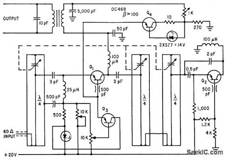
Two electronically regulated voltage sources are required to control current-tuned condition and collector voltage, using transistors OC468 and TF65 with zener diodes. One transistor operates in harmonic-generation mode as pump oscillator, comparable to parametric amplification.-U. L. Rhode, Pushing Transistors Above Their Frequency limits, Electronics, 35:25, p 46-49. (View)
View full Circuit Diagram | Comments | Reading(677)
SWITCHED_OVERTONE_CRYSTALS
Published:2009/7/6 0:57:00 Author:May

Uses third-overtone crystals between 20 and 80 MHz, with diode switching and with frequency doubling in transistors. L1-Ln ate series resonant with 10 pF at each crystal frequency. L4 is resonant with l0 pF at desired output frequency. L3 and L5 have one-third as many turns as L4. Q1 is 2N918, BF115, HEP709, or equivalent. Diodes are switching types such as BAY67.-U. Rohde, Stable Crystal Oscillators, Ham Radio, June 1975, p 34-37. (View)
View full Circuit Diagram | Comments | Reading(994)
1_kHz_V_FOR_VCO
Published:2009/7/6 0:55:00 Author:May

Voltage-contronea oscillator uses CA3130 opamp as MVBR and CA3160 opamp as comparator. Tracking error is about 0.02%, and temperature coefficient is 0.01% per degree C.- Circuit Ideas for RCA Linear ICs, RCA Solid State Division, Somerville, NJ, 1977, p4. (View)
View full Circuit Diagram | Comments | Reading(778)
STABLE_35_38_MHz_VFO
Published:2009/7/6 0:54:00 Author:May

Oscillator Q1-Q2, emitter-follower output Q3, and buffer Q4 provide 5 V P-P into 200-ohm load, with good isolation between oscillator and load Total drift is less than 10 Hz from turn-on, and less than 330 Hz as supply voltage varies between 15 and 30 V. Amplitude stability is within 1 dB over tuning range. Oscillator amplitude is stabilized by two 1N34 diodes and 3.3-V zener. L1 is 25 turns No. 18 closewound on 1.5-in form. –J. Fisk, Circuit sand Techniques, Ham Radio, June 1976, p 48-52. (View)
View full Circuit Diagram | Comments | Reading(816)
10_kHz_SINE_COSlNE
Published:2009/7/6 0:52:00 Author:May

Combination of SN72310 voltage-follower opamp and SN 72301A high-performance opamp gives two outputs differing in phase by 900. Supply is ±18 V.- The Linear and Interface Circuits Data Book for Design Engineers, Texas Instruments, Dallas, TX, 1973, p 4-40. (View)
View full Circuit Diagram | Comments | Reading(611)
160_METER_VFO
Published:2009/7/6 0:52:00 Author:May

Standard Colpitts oscillator Q1 with emitter-follower Q2 gives dependability and adequate isolation from later stages Zener regulation provides stability even with weak battery Output is about 0.7 VRMS. Low-level parasitic oscillation may occur about 150 kHz below operating frequency but is suppressed by tuned stages following VFO. L1 is 52 turns No. 28 enamel on Amidon T-50-2 toroid. RFC1 is 850μH.-A Weiss, Design Notes on a Moderate Power Solid State Transmitter for 1.8 MHz, CQ, Nov. 1972, p 18-22, 24, 98, 100, and 102. (View)
View full Circuit Diagram | Comments | Reading(1612)
3_20_MHz_CRYSTAL
Published:2009/7/6 0:51:00 Author:May

Circuit is series-mode oscillator, but parallel-mode crystals can be used if trimmer in series with crystal is replaced by short-circuit. Adjust feedback by varying ratio of C1 to C2. Use grid-dip oscillator to resonate L1 with C1 when crystal is shorted; then remove short and tune slug of L1 to pull crystal exactly to frequency. R1 should be between 100 and 1000 ohms. The lower its value, the lower the crystal power dissipation and the better is stability. Q1 is 2N918, 2N3564, 2N5770, BF200, SE1001, or equivalent.-R. Harrison, Survey of Crystal Oscillators, Ham Radio, March 1976, p 10-22. (View)
View full Circuit Diagram | Comments | Reading(2133)
SURE_STARTING_CRYSTAL
Published:2009/7/6 0:50:00 Author:May

Loop-within-a-loop oscillator design ensures reliable starting without use of critical components Frequency depends on crystal, which can be anywhere in range from 1 to 20 MHz IC can be 54L00 for 1-2 MHz、standard 54H00 for 2-6 MHz, and 54H00 or 54S00 for 6-20 MHz. Temperature stability is adequate for crystal clocks and other digital-system applications.-J. E. Buchanan, Crystal-Oscillator Design Eliminates Start-Up Problems, EDN Magazine, Feb. 20, 1978, p 110. (View)
View full Circuit Diagram | Comments | Reading(818)
LOW_DRIFT_7_MHz_VFO
Published:2009/7/6 0:48:00 Author:May

Low-drift solid-state design for 40-meter band has maximum change of only 25 Hz from cold start to full warm-up at 25℃. After stabilization, maximum hunting is 5 Hz. Drift is minimized by paralleling two or more capacitors in critical parts of circuit. Series-tuned Colpitts oscillator is followed by two buffer stages, with second providing enough amplification for practical amateur work while further improving isolation of oscillator. Low-impedance output network minimizes oscillator pulling from load changes. Article stresses importance of choosing and using components that minimize drift.-D. DeMaw, VFO Design Techniques for Improved Stability, Ham Radio, June 1976, p 10-17. (View)
View full Circuit Diagram | Comments | Reading(2267)
DUAL_FREOUENCY_CRYSTAL
Published:2009/7/6 0:46:00 Author:May

Uses two different crystals, with frequency being changed by reversing supply voltage,Transistor then inverts itself and gain reduces to about 2, which is adequate for oscillator operation Provides two frequencies from single stage with minimum of switching.-Circuits, 73 Magazine, Feb. 1974, p 101. (View)
View full Circuit Diagram | Comments | Reading(853)
IC_CRYSTAL
Published:2009/7/6 0:45:00 Author:May

Uses LM375 IC with crystals from 3 to 20 MHz in parallel mode. Will oscillate with only 4-V supply, but output voltage increases with supply voltage, L1 -C1 is resonant at crystal frequency. Adjust L1 only for maximum output, not for trimming frequency. If C3 is 3-30 pF, it can be used to adjust frequency of crystal.-R. Harrison, Survey of Crystal Oscillators, Ham Radio, March 1976, p 10-22. (View)
View full Circuit Diagram | Comments | Reading(850)
9_MHz_LINEAR_VCO
Published:2009/7/6 0:43:00 Author:May

U1A and U1C of RCA CA3046 transistor array form emitter-coupled oscillator. Portion of U1A current is diverted through U1B and L1, producing magnetic flux that reduces effective inductance of resonating coil L2. Output frequency is varied in direct pro portion to voltage applied at A. L1 is 23 turns on 3/4-inch Teflon form 2 inches long, with 4 turns wound between windings for L2. VR1 is 1N3828 6.2-V zener. Circuit must be well grounded and shielded to avoid hum pickup by input, which could modulate output.-D. G. Stephenson, A Second Look at Linear Tuning, OST, March 1977, p 40-41. (View)
View full Circuit Diagram | Comments | Reading(1389)
1_MHz_SERIES_MODE_CRYSTAL
Published:2009/7/6 0:42:00 Author:May

Motorola MC1553 video amplifier provides wide band-width and output swing capability needed for high-frequency master clock or local oscillator in many system designs. Positive feedback is injected through crystal to input pin 1. Output is taken from pin 7 which is buffered internally from oscillator by gain and emitter-follower stages. Brute-force pi filter at output extracts desired fundamental frequency.- A Wide Band Monolithic Video Amplifier, Motorola, Phoenix, AZ, 1973, AN-404 , p 9. (View)
View full Circuit Diagram | Comments | Reading(752)
| Pages:110/195 At 20101102103104105106107108109110111112113114115116117118119120Under 20 |
Circuit Categories
power supply circuit
Amplifier Circuit
Basic Circuit
LED and Light Circuit
Sensor Circuit
Signal Processing
Electrical Equipment Circuit
Control Circuit
Remote Control Circuit
A/D-D/A Converter Circuit
Audio Circuit
Measuring and Test Circuit
Communication Circuit
Computer-Related Circuit
555 Circuit
Automotive Circuit
Repairing Circuit