
Signal Processing
Index 108
THREE_PHASE_SQUARE_WAVE_OUTPUT_GENERATOR
Published:2009/7/6 19:56:00 Author:May
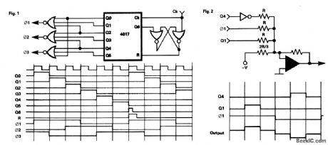
This circuit gives a 3 phase square-wave output for a variable speed motor drive.Operation is straightforward, the 4017 counter is synchronously reset after six clock inputs. The six outputs are combined to give the required waveforms. It is interesting to note that although NOR gates are shown, OR gates will give effectively the same result. The circuit can be extended as shown in Fig. 2 to give pseudo-sine waves if that is required, but that will diminish the simplicity of the circuit.
(View)
View full Circuit Diagram | Comments | Reading(1242)
LINE_FREQUENCY_SQUARE_WAVE_GENERATOR
Published:2009/7/6 19:55:00 Author:May

With only three components and a buffer, a line frequency square wave having a 1:1 duty cycle may be derived from the power supply. During the alternate half-cycle, however, A is effectively clamped to -0.7 V by Dl in the bridge which offsets the forward voltage across D2 giving an input to IC1 of approximately 0 V. When A rises above + 5 V, D2 is reverse biased and remains at +5 V. R1 is needed to load the transformer secondary maintaining a distortion-free waveform at A during the time the diode bridge is not conducting. C1 although not essential may be required to remove transients.
(View)
View full Circuit Diagram | Comments | Reading(727)
Voltage_controlled_ramp_generator_that_uses_a_PUT
Published:2009/7/22 4:01:00 Author:Jessie
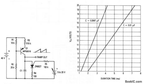
This circuit shows a PUT used as a VCRG. Figure 9-23B shows a plot of voltage-ver sus-ramp duration for two values of C1. (View)
View full Circuit Diagram | Comments | Reading(625)
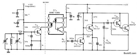
40_TO_43_MHz_VFO_CIRCUIT
Published:2009/7/22 3:59:00 Author:Jessie
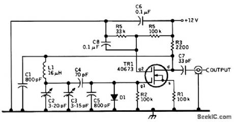
This is a recent 4.0- to 4.3-MHz oscillator design by KGBSU. It seems likely that performance could be improved by increasing the value of C2=C3 and decreasing that of L1 to make the device a true Vacker oscillator. The following component information is recommended by KGBSU: C1 and C5, 800-pF polystyrene; C2, air trimmer for setting calibration, C3, air variable for main tuning; C4, 70-pF, NPO ceramic and silver mica to provide required temperature compensation; C7, 33-pF NPO ce-ramic; C6 and C8, 0.1-μF 25-Vmonolithic capacitor; TR1, 40673 or SK3050 dual-gate MOSFET; D1, 1N4153 or 1N914 silicon signal diode; L1, 16-μF, 34 turns #26 enameled on 3/4-in diameter ceramic form (no slug core), winding length 0.6 inch; all resistors 0.25 W, 5 percent. (View)
View full Circuit Diagram | Comments | Reading(811)
HIGH_STABILITY_VFO
Published:2009/7/22 3:55:00 Author:Jessie
This circuit was published in the 1960s, but with moderndevices, it is still a useful design approach. The transistors are both 2N384. (View)
View full Circuit Diagram | Comments | Reading(660)
PORTABLE_RF_BURST_GENERATOR
Published:2009/7/6 9:04:00 Author:May

The circuit generates low-level rf bursts having frequencies as high as 10 MHz, thus permitting field testing of high frequency receivers. A jumper-selectable binary fraction (1/2 to 1/256 of the Y1 crystal frequency gates the output rf signal. Output amplitude (open circuit) is approximately 100 mV; output impedance is approximately 49Ω. The rf source is a clock oscillator based on a 3.58-MHz, color-burst crystal and two inverting buffers. The oscillator drives two cascaded 4-bit binary counters, IC2, and the sync signal resets the counters with a logic-high pulse-logic low at the counters. Select the desired output frequency by adding a jumper to one of the counter's eight output lines, which provides an enable signal for the two 3-state output buffers. The square-wave output at IC1, pin 11, is attenuated by R1, R2, and R3 to fix the output resistance at approximately 49Ω. Resistor R3 is the only critical component; for clean gating, isolate it from the rest of the circuit. (View)
View full Circuit Diagram | Comments | Reading(1215)
TWO_STATE_NEON_OSCILLATOR
Published:2009/7/6 9:02:00 Author:May
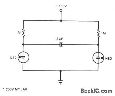
The number of lamps is easily increased in this oscillator. (View)
View full Circuit Diagram | Comments | Reading(591)
Photodetector_fiberoptic_receiver
Published:2009/7/22 4:25:00 Author:Jessie
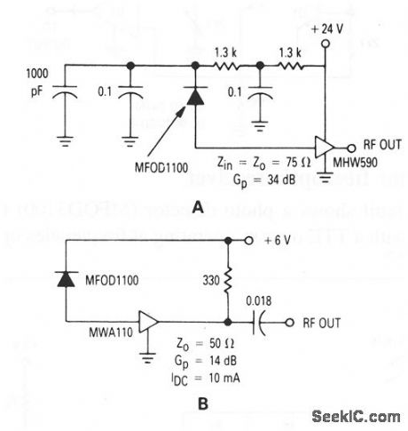
These circuits show a photo detector (MFOD1100) used as a fiberoptic receiver. (View)
View full Circuit Diagram | Comments | Reading(553)
INSULATION_RESISTANCE_TESTER
Published:2009/7/22 20:33:00 Author:Jessie
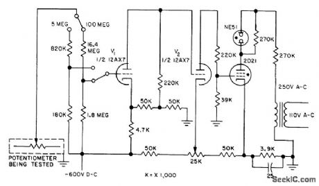
Amplifiers and thyratron give go-no-go indication of insulation resistance. Used in production testing of potentiometer-type pressure-sensing instruments over their operating ranges.-C. N. Boode and C. E. Calohan, Analog Comparator for Production Testing, Electronics, 31:13, p 47-49. (View)
View full Circuit Diagram | Comments | Reading(1909)
TUNNEL_DIODE_CURVE_TRACER
Published:2009/7/22 20:31:00 Author:Jessie
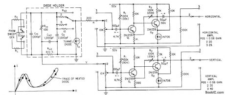
Diode holder uses germanium blocks as low-inductance resistors, for tracing negative-resistance region of tunnel diode. Heating effects may cause double trace.-H. G. Dill and M. It. Mac-Pherson, Tracing Tunnel Diode Curves, Electronics, 33:32, p 62-64.
(View)
View full Circuit Diagram | Comments | Reading(725)
TV_MIXER_TRANSISTOR_TESTER
Published:2009/7/22 20:27:00 Author:Jessie
Used as standarized test circuit for mixer transistors in tv and vhf receivers.-G. J. Flynn, Engineering Trends in Consumer Electronics, Electronics, 34:1, p 115-117. (View)
View full Circuit Diagram | Comments | Reading(486)
BASIC_MOS_OSCILLATOR
Published:2009/7/6 7:57:00 Author:May
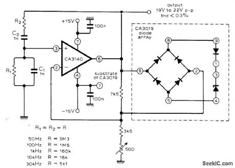
Output is 50 Hz when R1 and R2 are 3.3 megohms, increasing to 30 kHz as resistor values are reduced to 5100 ohms. Circuit has no inherent lower frequency limit; with 22-megohm resistors and 1-μF capacitors for C1 and C2, sine-wave output is 0.007 Hz. Articlegives basic equations for circuit. Features indude high input impedance, fast slew rate, and high output voltage capability. Combination of bridge rectifier with monolithic zener diodes in regulating system provides practically zero temperature coefficient.-M. Bailey, Op-Amp Wien Bridge Oscillator, Wire-less World, Jan. 1977, p 77. (View)
View full Circuit Diagram | Comments | Reading(652)
Darlington_photodetector_fiberoptic_recerver
Published:2009/7/22 6:05:00 Author:Jessie
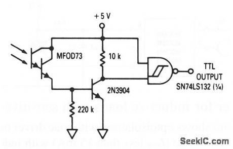
This circuit shows a Darlington photodetector (MFOD73) with a TTL output that operates at frequencies up to 1 kHz. (View)
View full Circuit Diagram | Comments | Reading(677)
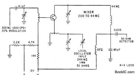
15_57_MHz_OPTICALLY_ISOLATED_VFO
Published:2009/7/6 7:46:00 Author:May
View full Circuit Diagram | Comments | Reading(733)
TUBE_LIFE_TEST_PULSER
Published:2009/7/22 20:54:00 Author:Jessie
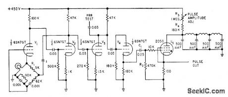
Pulse generator produces 0.25-microsec pulses at 50 v for life-testing of 1 to 15 microwave triodes at a time. Amplitude and repetition rate are adjustable within limits.-R. S. Ringland, Pulse Variable Works into Variable Load, Electronics, 31:37, p 102-103. (View)
View full Circuit Diagram | Comments | Reading(583)
__PHASE_TRACKING_THREE_PHASE_GENERATOR
Published:2009/7/6 7:27:00 Author:May
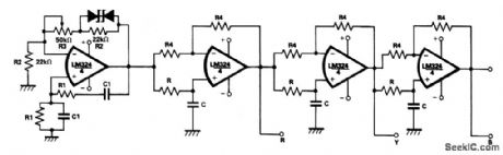
Using a single chip LM324 can, with active R-C networks, reduce the size of a 3-phase waveform generator, and prove useful in compact and stable 3-phase inverters. One quarter of an LM324 is used as a Wien bridge oscillator generating a pure sinusoidal waveform while the remaining parts of the LM324 are used as three 120° fixed phase shifters.Initially potentiometer R3 should be varied to adjust the loop gain of the oscillator in order to start the oscillator. (View)
View full Circuit Diagram | Comments | Reading(2742)
SQUARE_WAVE_OSCILLATOR
Published:2009/7/6 7:24:00 Author:May
View full Circuit Diagram | Comments | Reading(0)
DC_DC_OPTOISOLATOR
Published:2009/7/6 7:14:00 Author:May
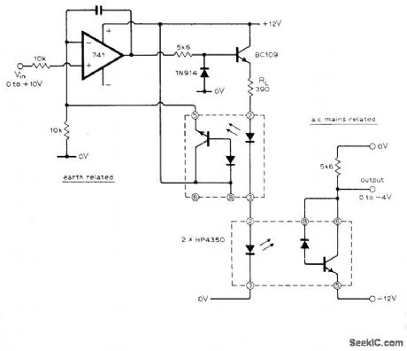
Designed to provide input isolation for thyristor converters. Linearity is within 2%. Loop gain of opamp makes diode turn-on voltage insignificant.-R. J. Haney, Linear D.C./D.C. Opto Isolator, Wireless World, June 1976, p 72. (View)
View full Circuit Diagram | Comments | Reading(976)
LOW_FREQUENCY_TTL_OSCILLSATOR
Published:2009/7/6 7:11:00 Author:May
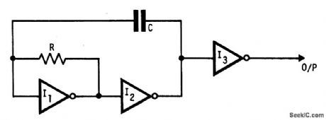
This oscillator uses standard inverters,one resistor and one capacitor,and has nommmlum operating frequency.R and C must be chosen such that currents into the gatesare below recommended operating limits and that leakage current into the gates andinto C are small h companson with the current in R also the output should be buffered(I3)to prevent variations h load affecting frequency.This circuit may also be used to square up slowly changing logic levels by use of multi input gates (NANDS,NORS Etc). (View)
View full Circuit Diagram | Comments | Reading(619)
Fast_optically_isolated_transistor_or_switch
Published:2009/7/22 22:28:00 Author:Jessie
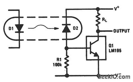
This circuit is similar to that of Fig. 9-54, but it has better ac response. The cathode of D2 is returned to a separate positive supply, rather than to the collector of Q1, which eliminates the added collector-to-base capacitance of D2. With this circuit, a 40-V 1-A load can be switched in 500 ns. Any photosensitive diode can be used for D2, instead of the optoisolator, to make a light-activated switch. (View)
View full Circuit Diagram | Comments | Reading(828)
| Pages:108/195 At 20101102103104105106107108109110111112113114115116117118119120Under 20 |
Circuit Categories
power supply circuit
Amplifier Circuit
Basic Circuit
LED and Light Circuit
Sensor Circuit
Signal Processing
Electrical Equipment Circuit
Control Circuit
Remote Control Circuit
A/D-D/A Converter Circuit
Audio Circuit
Measuring and Test Circuit
Communication Circuit
Computer-Related Circuit
555 Circuit
Automotive Circuit
Repairing Circuit