
Index 411
Crystal diode DDZX9689TTS internal circuit
Published:2011/5/23 21:03:00 Author:John | Keyword: Crystal diode
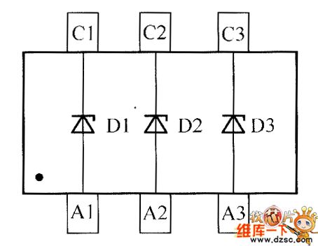
Crystal diode DDZX9689TTS internal circuit is shown below.
(View)
View full Circuit Diagram | Comments | Reading(424)
The motor dual insurance starter circuit diagram
Published:2011/5/21 0:58:00 Author:Lucas | Keyword: dual , insurance starter , motor
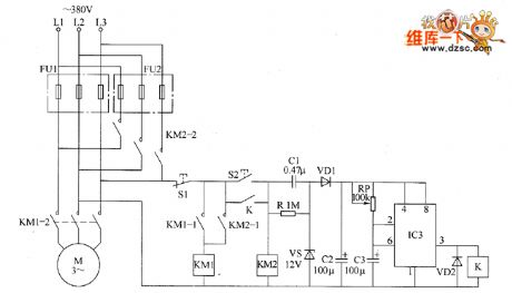
The motor dual insurance starter circuit is composed of the Road 1 fuse FU1, Road 2 fuse FU2, stop button R1, start button S2, AC contactors KM1, KM2, relay K, capacitors C1 ~ C3, diodes VD1, VD2, resistor R, voltage regulator diode VS, potentiometer RP and time-based integrated circuit IC, the circuit is shown as the chart. After people press the start button S2, KM2 pulls in and its normally open contacts KM2-i and KM2 ˉ 2 are connected, the motor M operates. At the same time, the AC voltage across L2, L3 is bucked by C1, stabilized by VS, filtered by VD1 and rectified by C2 to provide the +12 V power supply for IC. R uses 1W metal film resistor. RP selects small organic solid potentiometer or variable resistor. IC uses NE555 base integrated circuit.
(View)
View full Circuit Diagram | Comments | Reading(4289)
Motor decompression starter circuit diagram 2
Published:2011/5/21 23:32:00 Author:Lucas | Keyword: Motor decompression starter
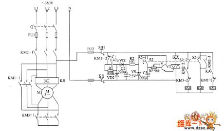
Motor decompression starter is composed of the power supply circuit, the delay control circuit and control implementation circuit, the circuit is shown as the chart. Power supply circuit is composed of the fuses FU1, FU2, stop button S1, capacitors C1, C2, the normally closed contacts of thermal relay KR , resistors R1, R2 and Zener diode VS. Delay control circuit is composed of the start control button S2 (S2-1 ~ S2-3), capacitor C3, potentiometer RP, transistors V, VT and intermediate relay KA. Control implementation circuit is composed of AC contactors KM1 ~ KM3, linkage contacts S2-2, S2-3 of qo and the normally open contacts of KA. AC 220V voltage is bucked by C1, rectified by VD1, filtered by C2, limited by R2 and stabilized by VS to produce the 7.5V DC voltage, which is added to the collector of V. R1 and R2 select 1/4W metal film resistors. RP uses synthetic carbon potentiometer.
(View)
View full Circuit Diagram | Comments | Reading(754)
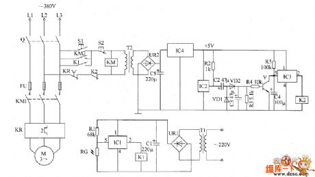
Motor decompression starter circuit diagram 1
Published:2011/5/21 23:21:00 Author:Lucas | Keyword: Motor decompression starter

Motor decompression starter is composed of decompression starting control circuit and protection circuit. the circuit is shown as the chart. Decompression starting control circuit is composed of the start button S1, the master controller (Q2a, Q2b), AC contactors KM1 ~ KM3, intermediate relays KA1, KA2, time relay KT, auto transformer TA1 and so on. Protection circuit consists of the power transformer T, the diodes VD1 ~ VD5, capacitors C1 ~ C3, three-terminal integrated voltage regulator integrated circuit IC1, potentiometer RP, time-base integrated circuit IC2 and relay Κ and so on. TA2, TA3 are the current transformers, KR1 and KR2 are the thermal relays, QS is the circuit breaker. C1 and C2 select the luminum electrolytic capacitors with voltage in 25V a; C3 and CZ choose monolithic capacitors. RP uses small potentiometer or variable resistor. VD1 ~ VD5 select 1N40071N rectifier diodes.
(View)
View full Circuit Diagram | Comments | Reading(2290)
Warping machine automatic controlled economizer circuit diagram
Published:2011/5/21 23:51:00 Author:Lucas | Keyword: Warping machine , automatic controlled, economizer
The warping machine automatic controlled economizerircuit consists of the light control circuit, magnetic circuit, +5 V power supply circuit and motor main control circuit, the circuit is shown as the chart. Light control circuit consists of photoresistor RC, resistor R1, electronic switch integrated circuit IC1, relay K1, filter capacitor Cl, bridge rectifier UR1 and power transformer T1. Magnetic circuit is composed of the Hall sensor integrated circuit IC2, resistors R2 ~ R5, electronic switch integrated circuit IC3, capacitors C2 ~ C4, diodes VD1, VD2, transistor V and relays K2. +5 V power supply circuit is composed of the power transformer T2, bridge rectifier UR2, filter capacitor C5 and three-terminal voltage regulator integrated circuit IC4. The motor main control circuit consists of knife switch Q, start button S1, stop button S2, fuse FU, AC contactor KM and thermal relay KR.
(View)
View full Circuit Diagram | Comments | Reading(1484)
Optical proximity switch circuit diagram
Published:2011/5/22 0:06:00 Author:Lucas | Keyword: Optical, proximity switch
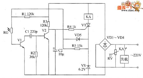
The optical proximity switch circuit consists of the photosensitive resistor RG, varistor RV, transistors V1 and V2, resistors R1 ~ R5, capacitors C1 and C2, voltage regulator diode VS, thyristor VT and diodes VD1 ~ VD5 etc. the circuit is shown as the chart. RV is the pressure sensitive resistor for protection to prevent the surge voltage shocks. During the turn-in VT, the 6V voltage on the VS can provide working power for the optical circuit by R7. R1 ~ R5 select 1/4W metal film resistors. RC uses the photosensitive resistor with light resistance being less than 20kΩ, the dark resistance being greater than 500kΩ . RV uses 270V varistor. C1 uses high-frequency ceramic capacitor or mica capacitor; C2 uses the aluminium electrolytic capacitor with the voltage in 16V. VD1 ~ VD5 use 1N4007 silicon rectifier diodes. VS selects 1N4735 (1W, 6.2V) silicon voltage regulator diode. V1 and V2 use 59013 silicon NPN transistor. VT uses MCR100-6 intergranular tube. KA uses intermediate relay with the coil voltage in DC 220V, and the current capacity on its contact should be based on rational power of load.
(View)
View full Circuit Diagram | Comments | Reading(1605)
Time relay circuit diagram 1
Published:2011/5/20 23:51:00 Author:Lucas | Keyword: Time relay
The relay circuit is composed of +12 V power supply circuit, oscillator circuit, delay trigger circuit and electronic switching circuit, the circuit is shown as the chart. +12 V power supply circuit consists of resistors R1 ~ R3, intermediate relay KA coil, diode VD1, Zener diode VS and filter capacitor C1. Oscillation circuit is composed of NOT gate IC (D1 ~ D6) within the NOT gates D5, D6, and capacitor C2, resistors R4 ~ R6, potentiometer RP1, diode VD2. Delay trigger circuit is composed of the IC within the NOT gates Dl, D2, D4, resistors R9, potentiometers RP2, RP3, capacitor C3 and diode VD3. Electronic switching circuit consists of intermediate relay KA, intergranular tube VT, resistors R7, R8 and capacitor C4.
(View)
View full Circuit Diagram | Comments | Reading(900)
Time relay circuit diagram 2
Published:2011/5/21 0:07:00 Author:Lucas | Keyword: Time relay
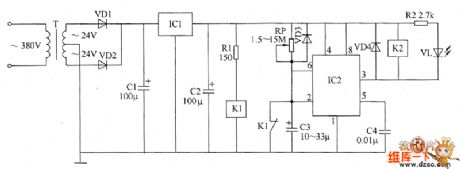
The relay circuit is composed of the power supply circuit, monostable circuit and relay control circuit, the circuit is shown as the chart. Power circuit is composed of the power transformer T, rectifier diodes VD1, VD2, three-terminal voltage regulator integrated circuit IC1 and filter capacitors C1, C2. Monostable circuit is composed of the potentiometer RP, diode VD3, capacitors C3, C4, time-base integrated circuit IC2 and the normally closed contact of relay K1. Relay control circuit consists of resistors R1, R2, relays K1, K2, diode VD4 and light emitting diode VL. R1 uses 1/2W metal film resistor; R2 uses 1/4W metal film resistor. RP uses organic, solid variable resistor. C1 uses aluminium electrolytic capacitor with the voltage in 50 V; C2 and C3 select aluminium electrolytic capacitor with the voltage in 13 V; C4 uses monolithic capacitor or polyester capacitor.
(View)
View full Circuit Diagram | Comments | Reading(841)
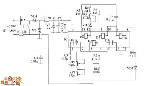
Time relay circuit diagram 3
Published:2011/5/21 0:24:00 Author:Lucas | Keyword: Time relay
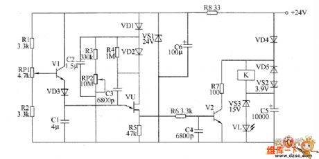
The relay circuit is composed of the regulator filter circuit, delay charging and discharging circuit and relay control circuit, the circuit is shown as the chart. Regulating filter circuit consists of resistor R8, zener diode VS and filter capacitor C6. Delay charging and discharging circuit consists of resistors R1 ~ R5, capacitors RP1 and RP2, transistor V1, capacitors Cl ~ C3, diodes VD1 ~ VD3 and single-junction transistor VU. Relay control circuit consists of resistors R6 and R7, capacitors C4 and C5, diodes VD4 and VD5, voltage regulator diodes VS2 and VS3, transistor V2, light-emitting diode VL and relay K. R1 ~ R6 select 1/4W metal film resistors; R7 uses 2W wirewound resistor; R8 selects 1/2W metal film resistor. RP1 uses multi-turn wirewound potentiometer; RP2 uses organic, solid potentiometer.
(View)
View full Circuit Diagram | Comments | Reading(763)
crystal diode DDZX9696TS internal circuit
Published:2011/5/20 5:34:00 Author:chopper | Keyword: internal circuit

View full Circuit Diagram | Comments | Reading(570)
crystal diode DDZX9694TS internal circuit
Published:2011/5/20 5:40:00 Author:chopper | Keyword: crystal diode, internal circuit

View full Circuit Diagram | Comments | Reading(520)
Automobile Gears Indicator
Published:2011/5/13 6:33:00 Author:Sue | Keyword: Automobile, Gears, Indicator
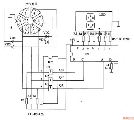
When the automobile is in neutral, S's 0 terminal is connected to the ground, the VD1-VD4 are disconnected. IC2's inside NOT gate D1-D3 output low level, and the LED indicator shows the number 0 .
When it's in gear 1, S's 1 terminal is connected to the ground, and NOT gate D3 will output high level. The indicator shows 1 .
When it's in gear 2, 2 terminal is connected to the ground, and NOT gate D1 will output high level. The indicator shows 2 .
When it's in gear 3, 3 terminal is connected to the ground, VD1 and VD2 are connected, NOT gate D1 and D3 will output high level. The indicator shows 3 .
When it's in gear 4, 4 terminal is connected to the ground, and NOT gate D2 will output high level. The indicator shows 4 .
When it's in gear 5, 5 terminal is connected to the ground, VD3 and VD4 are connected, NOT gate D2 and D3 will output high level. The indicator shows 5 . (View)
View full Circuit Diagram | Comments | Reading(1422)
MC14433-A/D Converting Integrated Circuit Diagram
Published:2011/5/21 21:46:00 Author:leo | Keyword: MC14433-A/D Converting Integrated Circuit Diagram
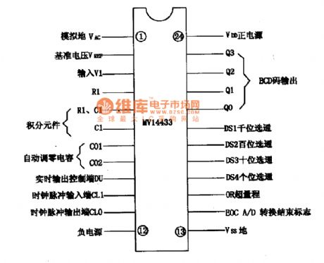
MC14433 is a kind of A/D converting integrated circuit produced by Motorola in USA which is widely applied in the multimeter that has a LED whose automatic range can show 3 1/2.
1.Function features:MC14433 contains a BCD code generating circuit, DS1-DS4 gate circuit of ones, tens, hundreds and thousands, A/D converting circuit, automatic zero set control circuit, voltage circuit of the base power supply as well as other related circuits.
2.Pins function and dataThe integrated circuit MC14433 adopts 24-pin dual line package. The arrangement and functions of its pins are as what is shown in the picture. (View)
View full Circuit Diagram | Comments | Reading(998)
MC68HSO5P4DW-Communication single chip microcomputer integrated circuit diagram
Published:2011/5/22 1:58:00 Author:leo | Keyword: MC68HSO5P4DW-Communication single chip microcomputer integrated circuit diagram

MC68HSO5P4DW is a kind of communication single chip microcomputer integrated circuit produced by Motorola in USA which is widely applied in wireless telephones.
1.Function features:The integrated circuit MC68HSO5P4DW is used to carry out impulse, two-tone compatible dial, input and output of various control signals, receiving detection and manually/automatically converting of various command signals.
2.Pin function and data:The integrated circuit MC68HSO5P4DW adopts 28-pin duel lie patch package. The picture gives the detailed information about its pin function and related data. (View)
View full Circuit Diagram | Comments | Reading(601)
temperature sensor compensation circuit
Published:2011/5/23 19:36:00 Author:John | Keyword: temperature sensor
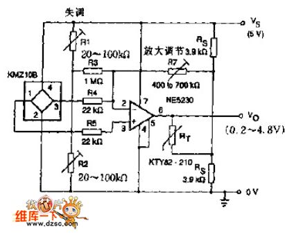
The sensor KTY series in the circuit is applied for positive or negative temperature drifting compensation. In many cases, temperature drifting of KMZ10B is negative. And an op-amp NE52300 is placed in the circuit to achieve the following functions:
1. Average (sensor to sensor) the sensitivity of temperature drift.2. Apply the potentiometer R1 and R2 for offset adjustment. 3. Use the potentiometer RT for gain adjustment.
(View)
View full Circuit Diagram | Comments | Reading(2606)
555 mini electronic massager circuit
Published:2011/5/23 6:53:00 Author:TaoXi | Keyword: mini, electronic massager
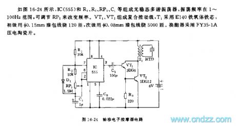
As the figure 16-24 shows, the astable multivibrator is composed of the IC(555) and R1,R2,RP1,C1, the oscillation frequency is between 1 to 100Hz, you can change the frequency by adjusting RP1. The composite promoting stage is composed of the VT1 and VT2, T1 uses the E140 ferrite core, the primary stage is binded with 120 turns of enamel insulated wire (the diameter is 0.15mm), the secondary stage is binded with 5000 turns of enamel insulated wire (the diameter is 0.08mm). The transducer uses the FY35-1A piezoelectric ceramic.
(View)
View full Circuit Diagram | Comments | Reading(1543)
555 acupuncture therapy and massage therapy instruments circuit
Published:2011/5/23 6:42:00 Author:TaoXi | Keyword: acupuncture therapy, massage therapy instruments
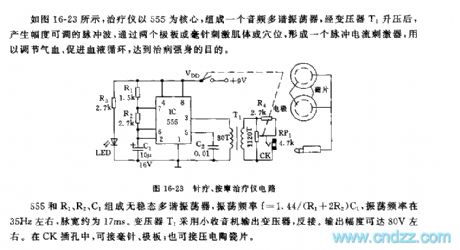
As the figure 16-23 shows, the treatment equipment uses the 555 as the core, and the audio multivibrator is composed of the 555, the signal is boosted by the transformer T1 and then produces the amplitude adjustable pulse.
The astable multivibrator is composed of the 555 and R1,R2,C1, the oscillation frequency f=1.44/(R1_2R2)C1, it is about 35Hz, the pulse width is about 17ms. The transformer T1 uses the small radio output transformer, and this transformer is reversed. The output amplitude is about 80V. You can connect the acupuncture needle, the counter electrode and the piezoelectric ceramics to the CK jack.
(View)
View full Circuit Diagram | Comments | Reading(1376)
Practical multi-function timer circuit
Published:2011/5/17 21:48:00 Author:TaoXi | Keyword: Practical, multi-function, timer
Practical multi-function timer circuit (View)
View full Circuit Diagram | Comments | Reading(474)
Toshiba CV60 (9.5~18.5kW) elevator main circuit
Published:2011/5/19 8:53:00 Author:TaoXi | Keyword: Toshiba, elevator, main circuit
Toshiba CV60 (9.5~18.5kW) elevator main circuit (View)
View full Circuit Diagram | Comments | Reading(433)
The air-bag and seatbelt control circuit of Buick-Century
Published:2011/5/18 2:31:00 Author:Borg | Keyword: air-bag, seatbelt, control circuit, Buick-Century
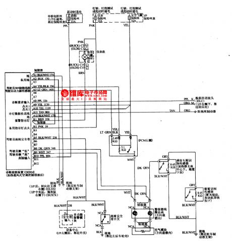
The air-bag is a kind of negative protection equipment, when the car is crashing with others in the running way, the sensor receives an impact signal, as long as it reaches a supposed degree, the sensor will generate a signal and send it to the controller, then the electric controller will compare it with the saved data. If it reaches the condition of opening the air-bag, the drive circuit will send a starting signal to the air generator of the air-bag module, and the generator will explode the gas-forming admixture and swell the air-bag.
(View)
View full Circuit Diagram | Comments | Reading(596)
| Pages:411/471 At 20401402403404405406407408409410411412413414415416417418419420Under 20 |
Circuit Categories
power supply circuit
Amplifier Circuit
Basic Circuit
LED and Light Circuit
Sensor Circuit
Signal Processing
Electrical Equipment Circuit
Control Circuit
Remote Control Circuit
A/D-D/A Converter Circuit
Audio Circuit
Measuring and Test Circuit
Communication Circuit
Computer-Related Circuit
555 Circuit
Automotive Circuit
Repairing Circuit