
Index 408
Water level indicator circuit (4)
Published:2011/5/29 22:55:00 Author:Christina | Keyword: Water level, indicator
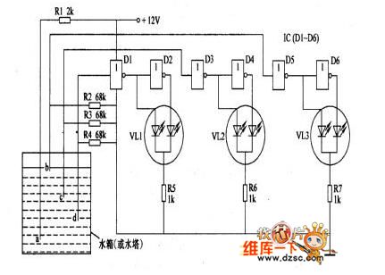
The operating principle: this circuit is composed of the water level detection circuit and the LED driving circuit, as the figure shows.
The water level detection circuit is composed of the water level detection electrodes a-d, the resistors Rl-R4, the Dl, D3, D5 of the NAND gate ICs Dl-D6.
The D driving circuit is composed of the IC, the discoloration LEDs LEDl-LED3 and the resistors R5-R7.
When the water level detection electrode d is in the water, the electrode connects with the electrode d through the resistance of water, the NAND gate Dl's input port has the high electrical level, and it's output port has the low electrical level, D2's output port has the high electrical level. When the water level is lower than the electrode d, Dl's input port has the low electrical level and the output port has the high electrical level, D2's output port has the low electrical level to make the VL1 to send out the red light. (View)
View full Circuit Diagram | Comments | Reading(1385)
Water level indicator circuit (2)
Published:2011/5/26 22:30:00 Author:Christina | Keyword: Water level, indicator

Circuit operating principle
This water level indicator circuit is composed of the water level detection electrode A-E, the four two-way analog switch integrated circuit IC, the light-emitting diode VLl-VM, the resistors Rl - R9, the audio amplifier tube V and the buzzer HA.etc, as the figure shows.
The electrode A is the low water level electrode; the electrode B is the 1/4 water level electrode, the electrode C is the 1/2 water level electrode, the electrode D is the 3/4 water level electrode; the electrode E is the high water level electrode.
When the water tank's water level is 1/4, the water resistance connects the electrode A with the electrode B, pin-13 of the IC has the high electrical level, the switch S1 of the IC opens to turn on the VL1.
(View)
View full Circuit Diagram | Comments | Reading(869)
Optical safety switch circuit diagram
Published:2011/5/30 6:28:00 Author:Lucas | Keyword: Optical safety switch
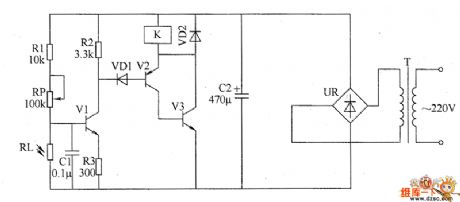
The optical safety switch circuit consists of the power supply circuit, light control circuit and control implementation circuit (switch circuit), the circuit is shown as the chart. Power circuit is composed of the power transformer T, bridge rectifier UR and filter capacitor C2. Light control circuit is composed of the photosensitive resistor RL, resistors R1 ~ R3, potentiometer RP, transistor V1 and capacitor C1. Control implementation circuit consists of the diodes VD1 and VD2, transistors V2 and V3 and the relay K. AC 220Y voltage bucked by T, filtered by UR and rectified by C2 can provide 6V DC voltage for light control circuit and control implementation circuit. R1 ~ R3 use potentiometer l/4W carbon or metal film resistors. RP selects variable potentiometer or solid film variable resistor.
(View)
View full Circuit Diagram | Comments | Reading(1537)
The inverter circuit diagram 2
Published:2011/5/30 4:31:00 Author:Lucas | Keyword: inverter
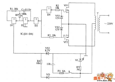
The inverter circuit consists of low-frequency oscillator, buffer and push-pull amplifier output circuit, the circuit is shown as the chart. Low-frequency oscillator is composed of two NOT gate circuits D1, D2 which is inside of NOT gate IC (D1 ~ D4), resistor R1, potentiometer RP and capacitor C. Buffer is composed of two NOT gate circuits D3, D4 which is inside of NOT gate IC (D1 ~ D4) and resistors R2, R3. Push-pull output circuit is composed of Zener diodes VS1, VS2, VM0S field-effect transistors VF1, VF2 and transformer T. Resistor R4, Zener diode VS3, diode VD and IC form the power supply circuit. Light-emitting diode V1, resistor R5 form the working indicating circuit. R1 ~ R5 use 1/4W carbon film resistors or metal film resistors.
(View)
View full Circuit Diagram | Comments | Reading(1093)
Eight-way lock electronic switch circuit diagram
Published:2011/6/1 7:00:00 Author:Lucas | Keyword: Eight-way , lock electronic switch
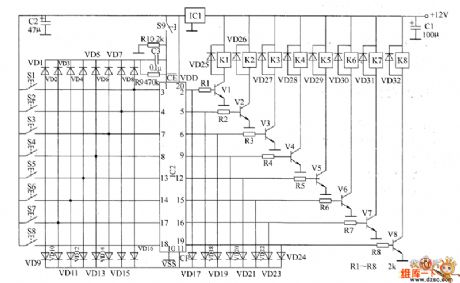
The 8-way lock electronic switch circuit is composed of the regulator filter circuit, input control circuit, latch circuit and control implementation circuit, and the circuit is shown as the chart. Regulator filter circuit is composed of the three terminal voltage regulator integrated circuit IC1 and filter capacitors C1, C2. Input control circuit consists of the control buttons S1 ~ S8, diodes VD1 ~ VD16. Latch circuit consists of eight D flip-flop integrated circuits IC2 and reset button S9, resistors R9 and R10, capacitor C3. Control implementation circuit is composed of the transistors V1 ~ V8, diodes VD17 ~ VD32, resistors R1 ~ R8 and relays K1 ~ K8. R1 ~ R10 uses 1/4W carbon film resistors or metal film resistors.
(View)
View full Circuit Diagram | Comments | Reading(1907)
Ultrasonic drilling machine circuit diagram 2
Published:2011/6/1 6:55:00 Author:Lucas | Keyword: Ultrasonic , drilling machine

The ultrasonic drilling machine circuit is composed of power supply circuit, ultrasonic oscillator circuit, preamplifier, promoting amplifier circuit and power amplifier output circuit, and the circuit is shown as the chart. Ultrasonic oscillator circuit consists of resistors R1 ~ R4, transistor V1, capacitors C1 ~ C4 and inductor L. Preamplifier circuit consists of transistors V1 ~ V5, resistors R5 ~ R15, potentiometer RP, capacitors C5 ~ C8 and C10 and the input transformer T1. Promoting amplifier circuit is composed of the input transformer T1, coupling transformer T2 and transistors V6, V7. Power amplifier output circuit is composed of the transistors V8 ~ V11, resistors R19 ~ R22, diodes VD1 ~ VD4, control switch S2, ammeter PA, output transformer T4 and transducers B.
(View)
View full Circuit Diagram | Comments | Reading(4594)
Ultrasonic drilling machine circuit diagram 1
Published:2011/6/1 6:48:00 Author:Lucas | Keyword: Ultrasonic, drilling machine

The ultrasonic drilling machine circuit is composed of power supply circuit, ultrasonic oscillator circuit, driver amplifier circuit and power output circuit, and the circuit is shown as the chart. Power circuit consists of the power switch S, power transformer T1, rectifier diodes VD1 ~ VD8, three-terminal voltage regulator integrated circuit IC and filter capacitors C1, C3, C5, C6. Ultrasonic oscillator circuit consists of resistors R9, R11, R12, inductor L, capacitors C7 ~ C9 and transistor V7. Driver amplifier circuit is composed of capacitor C4, transistors V8 and V9, input transformer T2 and resistors R7, R10, R13, R14. Power output circuit consists of the windings W2 and W3, transformer T2, power amplifier tubes V1 ~ V6, resistors R1 ~ R6, output transformer T3, capacitor C2 and ultrasonic transducer B.
(View)
View full Circuit Diagram | Comments | Reading(4797)
Mining charging indicator circuit diagram
Published:2011/6/2 4:04:00 Author:Lucas | Keyword: Mining , charging indicator
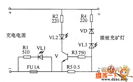
Mining charging indicator circuit consists of the resistors R1 ~ R5, light-emitting diode Ⅴ and fuse FU, and the circuit is shown as the chart. When the battery is charging, V is turned on, VL2 is lit. When the polarity connection of batteries is right, VL3 does not shine. If the battery polarity is reversed, the VL3 will be lit and emit yellow warning signal. When the fuse FU is fused because of some reasons (such as the internal battery short circuit), VL1 is lit. R1 ~ R4 select 1/4W metal film resistors; R5 uses 2 \ 7 wirewound resistor. VD selects 1N4007 silicon rectifier diode. VL1 ~ VL3 select φ5mm high-brightness light emitting diodes. V uses 58050 silicon NPN transistor.
(View)
View full Circuit Diagram | Comments | Reading(2016)
Xunda MB-DS elevator floor indicating circuit
Published:2011/6/2 1:33:00 Author:TaoXi | Keyword: Xunda, elevator, floor indicating
Xunda MB-DS elevator floor indicating circuit (View)
View full Circuit Diagram | Comments | Reading(459)
Xunda MB-DS elevator safety loop circuit
Published:2011/6/2 1:39:00 Author:TaoXi | Keyword: Xunda, elevator, safety loop
Xunda MB-DS elevator safety loop circuit (View)
View full Circuit Diagram | Comments | Reading(517)
Xunda MB-DS elevator main circuit
Published:2011/6/2 1:34:00 Author:TaoXi | Keyword: Xunda, elevator, main circuit
Xunda MB-DS elevator main circuit (View)
View full Circuit Diagram | Comments | Reading(464)
Xunda VFP elevator safety loop circuit
Published:2011/6/2 1:44:00 Author:TaoXi | Keyword: Xunda, elevator, safety loop
Xunda VFP elevator safety loop circuit (View)
View full Circuit Diagram | Comments | Reading(479)
Xunda VFP elevator dot-matrix internal choice button circuit
Published:2011/6/2 1:43:00 Author:TaoXi | Keyword: Xunda, elevator, dot-matrix, internal, choice button
Xunda VFP elevator dot-matrix internal choice button circuit (View)
View full Circuit Diagram | Comments | Reading(961)
Xunda elevator main circuit
Published:2011/6/2 1:42:00 Author:TaoXi | Keyword: Xunda, elevator, main circuit
Xunda 300P elevator main circuit (View)
View full Circuit Diagram | Comments | Reading(549)
Xunda VFP elevator dot-matrix outside call button circuit
Published:2011/6/2 1:43:00 Author:TaoXi | Keyword: Xunda, elevator, dot-matrix, outside, call button
Xunda VFP elevator dot-matrix outside call button circuit (View)
View full Circuit Diagram | Comments | Reading(551)
Xunda VFP elevator main circuit
Published:2011/6/2 1:44:00 Author:TaoXi | Keyword: Xunda, elevator, main circuit
Xunda VFP elevator main circuit (View)
View full Circuit Diagram | Comments | Reading(439)
Digital display electronic clock circuit
Published:2011/5/26 7:13:00 Author:Christina | Keyword: Digital display, electronic clock

This electronic clock is composed of the LM8365 and the LDD640R displayers. The LM8365 can display the hour/minute and month/day .etc; you can set two alarm ouptuts AD1 and AD2 by pressing 12h or 24h; VDD=-21 to -6.5V, it directly drives the LED displaying; this circuit has the function of subtraction timing; when the power cuts off or there is something wrong with the circuit, it has the function of all-bit flashing display. The LDD640R can use the 5V AC half wave rectification method to supply the power, in the full light state, the current is less than 200mA.
(View)
View full Circuit Diagram | Comments | Reading(5114)
Character display type logic pen circuit (CD4069) composed of the gate circuit (1)
Published:2011/5/26 7:31:00 Author:Christina | Keyword: Character display, logic pen, gate circuit
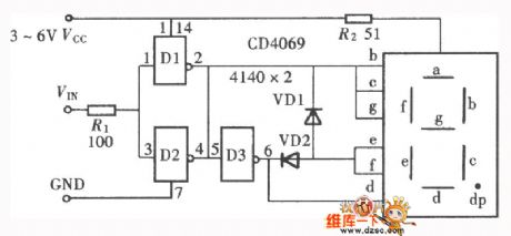
The character display type logic pen is as shown, here the characters are not our chinese characters 高 and 低 , they are the english characters H and L . For the particularity of the two characters' glyph, and this particularity is the same as the LED digital tube's pen section, so we are easy to use it to form the logic level test pen.
(View)
View full Circuit Diagram | Comments | Reading(781)
Anti-theft alarm telephone system circuit
Published:2011/6/1 20:50:00 Author:Christina | Keyword: Anti-theft, alarm telephone, system circuit
Anti-theft alarm telephone system circuit (View)
View full Circuit Diagram | Comments | Reading(473)
Baby sleep state monitor circuit
Published:2011/6/1 20:17:00 Author:Christina | Keyword: Baby, sleep state, monitor
The Baby sleep state monitor circuit (View)
View full Circuit Diagram | Comments | Reading(506)
| Pages:408/471 At 20401402403404405406407408409410411412413414415416417418419420Under 20 |
Circuit Categories
power supply circuit
Amplifier Circuit
Basic Circuit
LED and Light Circuit
Sensor Circuit
Signal Processing
Electrical Equipment Circuit
Control Circuit
Remote Control Circuit
A/D-D/A Converter Circuit
Audio Circuit
Measuring and Test Circuit
Communication Circuit
Computer-Related Circuit
555 Circuit
Automotive Circuit
Repairing Circuit