
Index 409
MC68HCO5C4P-Communication single-chip microcomputer integrated circuit diagram
Published:2011/6/1 22:24:00 Author:leo | Keyword: MC68HCO5C4P-Communication single-chip microcomputer integrated circuit diagram
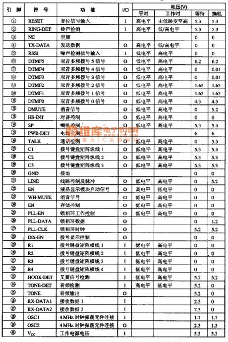
MC68HCO5C4P is a kind of communication single-chip microcomputer integrated circuit made by Motorola which can be applied in wireless telephone and is used as host control chip in cell phone.
1.Function Feature:The integrated circuit MC68HCO5C4P has one more 'P' than MC68HCO5C4. But they have part of different pins and cannot change directly for the same usage.MC68HCO5C4P is improved on the base of MC68HCO5C4. So most of functions of them are similar which can be found in the introduction of MC68HCO5C4 functions.
2.Pin Functions and dataThe integrated circuit MC68HCO5C4P adopts 40-pin package and is used together with MC68HC5PI. All pins function and data of the integrated circuit are shown in the picture bellow. (View)
View full Circuit Diagram | Comments | Reading(646)
Biploar Current Sources Circuit Diagram of Optical Coupler
Published:2011/5/20 20:12:00 Author:leo | Keyword: Biploar Current Sources Circuit Diagram of Optical Coupler, PS2501
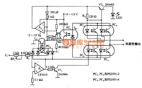
In the picture, there is a bipolar current sources circuit of optical coupler which consists of two operational amplifiers and four optical couplers. It is used to control the floating bridge output port using the battery for power supply, which is made up of PC3 to PC6.Its feature is to get the bipolar output current sources from single battery UB and adopt single-channel optical coupler PC1 as the control circuit of current output. At the same time, it is also used to improve the output polarity when output current is symmetric. (View)
View full Circuit Diagram | Comments | Reading(930)
555 multi-function appliance socket circuit (1)
Published:2011/6/1 3:06:00 Author:TaoXi | Keyword: 555, multi-function, appliance, socket
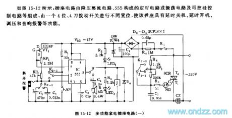
As the figure 15-12 shows, the socket circuit is composed of the step-down rectifier circuit, the timing circuit or oscilation circuit which is composed of the 555, and the silicon-controlled rectifier control circuit.etc, this circuit is set by a 4-bit, 4 knives switch, this socket has the function of delay shutdown, delay starting up, voltage adjustment and sound alarm.
The step-down rectifier circuit supplies the voltage of VDD=+12V to the controller. If you cut off K1 and dial down the K2-3, then adjust RP3, so you can adjust the conduction angle of the SCR and adjust the output voltage.
The 555 and R4,RP1,RP2,C3,C4,VT1 can form the timing boot or timing shutdown circuit, also they form the constant-current source recharging Much harmonic oscillator and the sound alarm circuit.
(View)
View full Circuit Diagram | Comments | Reading(536)
555 multi-function appliance socket circuit (2)
Published:2011/6/1 3:27:00 Author:TaoXi | Keyword: 555, multi-function, appliance, socket
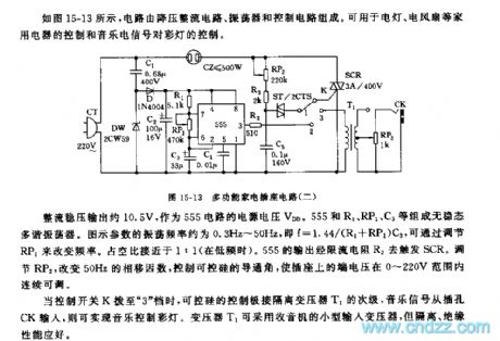
As the figure 15-13 shows, the circuit is composed of the step-down rectifier circuit, the oscillator and the control circuit. This circuit can be used in wide range of applications such as the electric lamp control, the electric fan control and the color lights control.
The rectifier voltage stabilization output is about 10.5V, this output can be used as the 555 circuit's power supply voltage VDD. The astable multivibrator is composed of the 555 and R1, RP1, C3. The figure parameters' oscillation frequency is about 0.3Hz~50Hz, f=1.44/(R1+RP1)C3, you can change the frequency by adjusting the RP1. The duty ratio is about 1:1. The output of 555 triggers the SCR through the current limiting resistor R2. By adjusting RP2 and changing the 50Hz phase shift factors, you can control the conduction angle of the SCR to make the terminal voltage in the range of 0~220V.
(View)
View full Circuit Diagram | Comments | Reading(475)
555 multi-function power supply socket circuit
Published:2011/6/1 3:52:00 Author:TaoXi | Keyword: 555, multi-function, power supply, socket
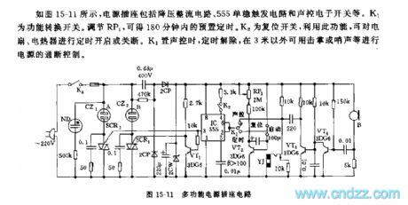
As the figure 15-11 shows, the power supply socket is composed of the step-down rectifier circuit, the 555 monostable trigger circuit and the sound control electronic switch.etc. K1 is the function conversion switch. You can get the preset timing in 180 minutes by adjusting RP1. K2 is the reset switch, you can timing open or close the fans and electric heaters by using K2. When K1 is on the sound control gear, the timing is removed, you can control the power supply on-off by the clapping or whistle three meters away.
(View)
View full Circuit Diagram | Comments | Reading(507)
555 ding-dong audio electronic doorbell circuit
Published:2011/6/1 4:04:00 Author:TaoXi | Keyword: 555, ding-dong, audio, electronic, doorbell
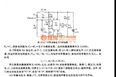
This two-tone bell circuit uses one piece of 555 time base circuit as the core. It sends out the beautiful and sweet sound of dingdong . The circuit is as shown in figure 15-46.
The multivibrator is composed of the 555 and R1~R3,D1,D2,C2. SA is the button switch of the door, it is usually in the disconnect state. When SA is closing, pin-4 of 555 has the low electric potential to keep it in the mandatory reset state, pin-3 outputs the low electric potential. When someone presses the SA, the power supply VDD will charge the C1 through SA and D1, pin-4 of 555 has the high electric potential, the 555 starts working, the vibration frequency fc1=1.44/(RD+2R3)C2.
RD is the DC resistance of D1 and D2.
(View)
View full Circuit Diagram | Comments | Reading(3169)
Internal circuit of the crystal transistors EMB6 and UMB6N
Published:2011/5/26 8:24:00 Author:Christina | Keyword: Internal circuit, crystal transistors
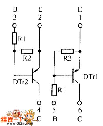
The Internal circuit of the crystal transistors EMB6 and UMB6N is as shown:
(View)
View full Circuit Diagram | Comments | Reading(483)
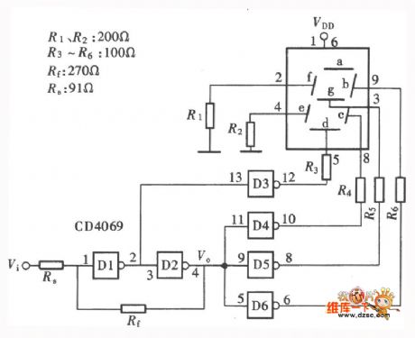
Shining type logic pen circuit (CD4069) composed of the gate circuit
Published:2011/5/26 6:54:00 Author:Christina | Keyword: Shining type, logic pen, gate circuit
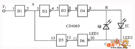
The logic pen also called the logic detection probe, it is the common tool to detect the various point's logical state of the digital circuit. The digital circuit has three kinds of logical state: the high electrical level 1 , the low electrical level 0 and the high resistance state . The test result of the logical state can be displayed by the LED and the sounder, also you can use the digital led to display it. The logic detection pen which is composed of the six inverter CD4069 and the LED is as shown in the figure.
(View)
View full Circuit Diagram | Comments | Reading(777)
Strip graphics display circuit
Published:2011/5/26 2:50:00 Author:Christina | Keyword: Strip, graphics, display circuit
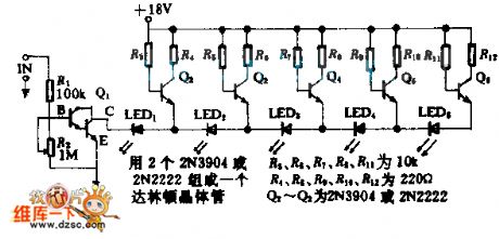
The transistor Q2~Q3 control the LED1~LED5 as the rise strip display of the input voltage. If you adjust the R2, the voltage minimum change range is 0.1~0.5V, the increment of the five LEDs is 0.1V; the voltage maximum change range is 1~10V, the increment is 1V. The input resistance of the circuit is more than 100KΩ.
(View)
View full Circuit Diagram | Comments | Reading(584)
Logarithmic operation circuit
Published:2011/5/26 2:45:00 Author:Christina | Keyword: Logarithmic, operation
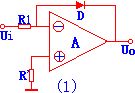
The logarithmic operation circuit makes the output voltage and the input voltage present the logarithm function. We replace the Rf of the inverse proportion circuit with the diode or the transistor to form the logarithmic operation circuit. The circuit is as shown:
(View)
View full Circuit Diagram | Comments | Reading(441)
133MHz multi-channel output clock pulse driving circuit
Published:2011/5/19 20:45:00 Author:Christina | Keyword: 133MHz, multi-channel, output clock, pulse driving circuit
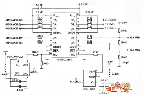
The 133MHz multi-channel output clock pulse driving circuit is as shown. It uses the clock pulse driving circuit which is composed of the P149FC32805, the maximum clock frequency is 133 MHz, and it can be used to distribute the base board internal clock signal. Output delay time is less than 270ps for synchronous management.
(View)
View full Circuit Diagram | Comments | Reading(587)
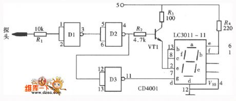
Character display type logic pen circuit (CD4011) composed of the gate circuit (2)
Published:2011/5/26 7:36:00 Author:Christina | Keyword: Character display, logic pen, gate circuit
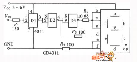
The character display type logic pen which is composed of the gate circuit has various forms, it can be composed by the inverter or the NAND gate, and also the NOR gate. The logic pen in the figure is composed of the NAND gate CD4011 and the common anode digital tube.
(View)
View full Circuit Diagram | Comments | Reading(1792)
Character display type logic pen circuit (CD4069) composed of the gate circuit (3)
Published:2011/5/26 7:38:00 Author:Christina | Keyword: Character display, logic pen, gate circuit
The Character display type logic pen circuit (CD4069) composed of the gate circuit (3) is as shown:
(View)
View full Circuit Diagram | Comments | Reading(883)
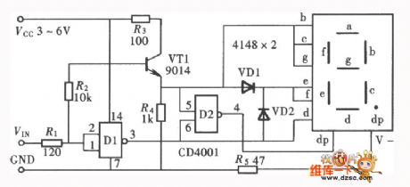
Character display type logic pen circuit (CD4001) composed of the gate circuit (4)
Published:2011/5/26 7:42:00 Author:Christina | Keyword: Character display, logic pen, gate circuit
The Character display type logic pen circuit (CD4001) composed of the gate circuit (4):
(View)
View full Circuit Diagram | Comments | Reading(1954)
Open-circuit state display logic pen circuit (CD4001) (1)
Published:2011/5/26 8:03:00 Author:Christina | Keyword: Open-circuit state, display, logic pen
The figure shows the logic pen that can test and display the high and low electrical level and the open-circuit state.
(View)
View full Circuit Diagram | Comments | Reading(1770)
Open-circuit state display logic pen circuit (2)
Published:2011/5/26 8:04:00 Author:Christina | Keyword: Open-circuit, state, display, logic pen

The Open-circuit state display logic pen circuit (2)
(View)
View full Circuit Diagram | Comments | Reading(592)
Lithium battery constant voltage charging circuit
Published:2011/5/30 21:21:00 Author:Fiona | Keyword: Lithium battery, constant voltage
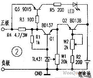
The figure below shows a constant current of the lithium battery charging control panel, the figure Q1, R1, W1, TL431 consist of the precision adjustable voltage circuit. Q2, W2, R2 consist of adjustable constant-current circuit. Q3, R3, R4, R5, LED are charging instructions circuit. With Rechargeable lithium battery's voltage rises gradually, charge current will gradually decrease,the R4 batteries voltage will continue to decrease after the battery is full finally ended Q3, LED is off, in order to ensure the battery is sufficient,please continue to charge 1 ~ 2 hours after the lights extinguished , it need to install the appropriate size of the heat sink at Q2, Q3 when using. (View)
View full Circuit Diagram | Comments | Reading(996)
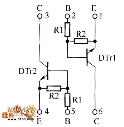
Crystal transistors EMD12 and UMD12N interal circuit
Published:2011/5/26 8:16:00 Author:Christina | Keyword: Crystal transistors, interal circuit
The Crystal transistors EMD12 and UMD12N interal circuit is as shown:
(View)
View full Circuit Diagram | Comments | Reading(655)
LED tuning indication circuit
Published:2011/5/25 22:11:00 Author:Christina | Keyword: LED, tuning, indication circuit
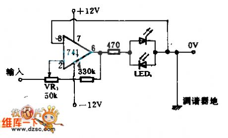
You can install a LED on the first endpoint of the tuning dish. Which light-emitting diode conducts, the tuning instruction will be away from it, when the two LEDs are all cut off, the tuning instruction will goes to dead point, so we get the right tuning instruction point.
The advantage of the tuner is the low current consumption, you can use a LED which has the weakest light to indicate the very tiny tuning error. By adjusting VR1, you can make the dead point area wide enough, so the LED will not flash because of the big volume language or music.
(View)
View full Circuit Diagram | Comments | Reading(563)
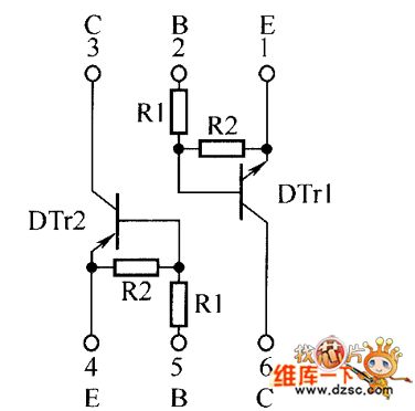
Internal circuit of the crystal transistors EMH9 and UMH9N
Published:2011/5/25 22:13:00 Author:Christina | Keyword: Internal circuit, crystal transistors
The internal circuit of the crystal transistors EMH9 and UMH9N is as shown:
(View)
View full Circuit Diagram | Comments | Reading(464)
| Pages:409/471 At 20401402403404405406407408409410411412413414415416417418419420Under 20 |
Circuit Categories
power supply circuit
Amplifier Circuit
Basic Circuit
LED and Light Circuit
Sensor Circuit
Signal Processing
Electrical Equipment Circuit
Control Circuit
Remote Control Circuit
A/D-D/A Converter Circuit
Audio Circuit
Measuring and Test Circuit
Communication Circuit
Computer-Related Circuit
555 Circuit
Automotive Circuit
Repairing Circuit