
Circuit Diagram
Index 1475
Electronic mosquito killer
Published:2011/7/24 22:38:00 Author:Ecco | Keyword: Electronic mosquito killer

The electronic mosquito killer circuit is composed of the energy-saving lamp circuit and high-voltage generator circuit, and the circuit is shown in Figure 3-196. Energy saving lamp circuit is composed of the rectifier diodes VDl-VD6, transistors Vl, V2, resistors Rl-R6, capacitors Cl-C6, pulse transformer T, choke L and black fluorescents ELl, EL2. The high-voltage generator circuit consists of resistors R7-RlO, capacitors C7-ClO, rectifier diodes VD7-VDl8 and high electrodes. Rl-RlO choose the 1/4W carbon film resistors or metal film resistors. Cl uses aluminum electrolytic capacitor with the voltage in 400V.
(View)
View full Circuit Diagram | Comments | Reading(13625)
Water Activated Alarm
Published:2011/7/24 22:33:00 Author:Ecco | Keyword: Water Activated Alarm

The circuit uses a 555 timer wired as an astable oscillator and powered by the emitter current of the BC109C. Under dry conditions, the transistor will have no bias current and be fully off. However as the probes get wet the transistor will conduct and sounding the alarm.An On/Off switch is provided and remember to use a non-reactive metal for the probe contacts. Gold or silver plated contacts from an old relay may be used, however a cheap alternative is to wire alternate copper strips from a piece of veroboard. These will eventually oxidize over but as very little current is flowing in the base circuit, the higher impedance caused by oxidization is not important. No base resistor is necessary as the transistor is in emitter follower, current limit being the impedance at the emitter (the oscillator circuit). (View)
View full Circuit Diagram | Comments | Reading(1)
Multi-waveform signal generator composed of 555
Published:2011/7/24 22:31:00 Author:Ecco | Keyword: Multi-waveform signal generator
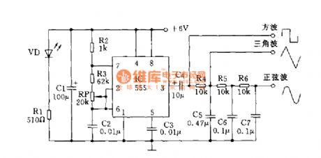
View full Circuit Diagram | Comments | Reading(4779)
Single-chip test board circuit 5
Published:2011/7/24 22:30:00 Author:Ecco | Keyword: Single-chip , test board

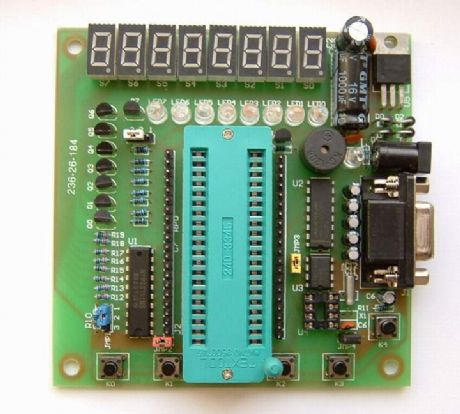

Jumper JMPO's role: it is used for the digital test unit and water light testing unit conversion, when it is short connected at the location of 12, the water light unit is effective; when it is short connected in the 23 position, the digital control unit is effective. Jumper JMP1's role: it is used to control the output enable of 74LS244 driver, when it is short connected in position 12, the enable is in the default location of the experimental board; when it is short connected at 23 position, all the output of the 74LS244 is in the low level, and it is no longer controlled by the microcontroller output. (View)
View full Circuit Diagram | Comments | Reading(961)
555 shooting game machine circuit
Published:2011/7/18 5:21:00 Author:nelly | Keyword: shooting game machine
The astable multivibrator is composed of IC3 and R5, R6, R3, C5, the oscillation frequency f=1.44(R5+2R6)C5, it is about 1000Hz. At the same time, The output of IC3 is made as the trigger pulse of SCR1~SCR5 by D2, R7. K1~K5 are made into target, when the bullet hits it , the relevant switch is connected, then the relevant SCR is triggered. Only SCR1~SCR5's G pole is triggered in order, LED2~LED6 will light. When IC1's timing time(60s)is ended, IC2 is sealed by the low level which is outputed by 555, IC2 is in forced reset state. At the same time, IC1 chip's discharge lamp is in short-circuit condition, even if it bits the target, SCR will not be triggered and turned on.
(View)
View full Circuit Diagram | Comments | Reading(688)
555 acoustic control electronic cat
Published:2011/7/18 5:23:00 Author:nelly | Keyword: acoustic control, electronic cat
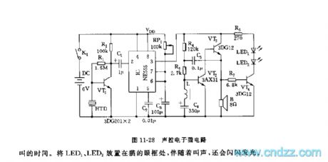
The monostable trigger delay circuit is composed of 555 and RP1, C3. The sudden burst sound(such as clap)is changed into electrical signal by piezoceramics HTD, then it is amplified and added to 555's trigger terminal's 2 foot by VT1. Due to VT1 is saturation conduction, 2 foot's level is lower than 1/3 VDD trigger level, 555 is set, it outputs(3 foot)high level, the audio frequency oscillator obtains electricity and starts to oscillate which is composed of VT2, VT3, L, C4, C5. The oscillation time is decided by 555 monostable delay time td. td depends on the time constant of RP1, C3. After 555 circuit is set, C3 is charged by RP1, when C3's voltage is higher than 2/3 VDD, 555 is reset again, 3 foot turns into low level, the oscillator is no electricity, and it stops oscillating, the cat's noise is stopped.
(View)
View full Circuit Diagram | Comments | Reading(1387)
Computer motherboard circuit 810 4_22
Published:2011/7/24 22:18:00 Author:Ecco | Keyword: Computer motherboard

View full Circuit Diagram | Comments | Reading(510)
Computer motherboard circuit 810 4_21
Published:2011/7/24 22:18:00 Author:Ecco | Keyword: Computer motherboard

View full Circuit Diagram | Comments | Reading(504)
Computer motherboard circuit 810 4_20
Published:2011/7/24 22:17:00 Author:Ecco | Keyword: Computer motherboard

View full Circuit Diagram | Comments | Reading(443)
The 555 blinking electronic cat circuit
Published:2011/7/18 5:23:00 Author:nelly | Keyword: blinking, electronic cat
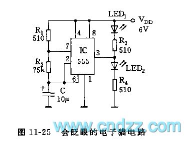

As shown on the figure 11-25, the astable multivibrator consists of the 555 and R1 and R2 and C. f=1.44/(R1 +2R2)C, the oscillation frequency on the figure is about 1Hz, the duty ratio is 50%. The high power level which outputs drives LED1 and the low power drives the LED2 drives the LED2. The LED1 and LED2 can light in turn. The R3 and R4 are Current-limiting protective resistances.
(View)
View full Circuit Diagram | Comments | Reading(465)
Computer motherboard circuit 810 4_19
Published:2011/7/24 22:17:00 Author:Ecco | Keyword: Computer motherboard

View full Circuit Diagram | Comments | Reading(466)
555 precautionary type electric leakage automatic protector circuit
Published:2011/7/18 5:27:00 Author:nelly | Keyword: precautionary type, electric leakage, automatic protector
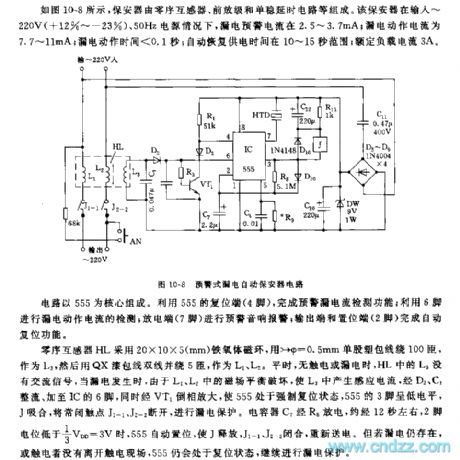
As shown in the figure 10-8, the protector is composed of zero-sequence transformer, preamplifier stage and monostable dalay circuit. In the context of the protector's input is 220V(+12%~-23%), 50Hz, the electric leakage warning current is between 2.5~3.7mA; the electric leakage action current is 7.7~11mA; the electric leakage action time is lower than 0.1s; the automatic recovery power supply time is between 10~15s; the rated load current is 3A.
The circuit is composed as the core of 555. It uses 555's reset terminal(4 foot), then can accomplish the testing function of precautionary current leakage; It uses 6 foot to do the testing of electric leakage; electric discharge terminal(7 foot) does the precautionary audio alarming; the output terminal and set terminal(2 foot)accomplish the automatic reset function.
(View)
View full Circuit Diagram | Comments | Reading(844)
555 indication circuit of monitoring battery undervoltage condition
Published:2011/7/18 5:27:00 Author:nelly | Keyword: monitoring battery, undervoltage condition, indication circuit
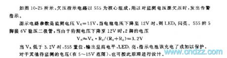
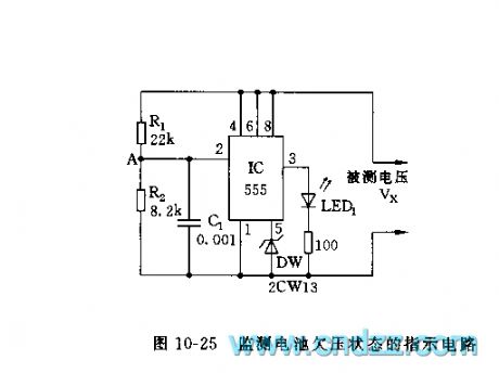
As shown in the figure 10-25, undervoltage indication circuit is composed as the core of 555, when the monitoring voltage is undervoltage, it will send out alarm indication. In the figure, the circuit parameter is the monitoring voltage Vx=15v, when the battery voltage drops to 12V, LED1 turns on. 555's 5 foot is connected to 6V Zener diode, when the measured voltage drops, 2 foot's voltage VA≈Vx·R2/(R1+R2)=3.2v. When VA is lower than 3.2V, 555 is set, the output is high level, LED1 turns on, it shows that the battery should be charged or protected. For other monitored voltages(in the range of 5~15V), they also can be designed as this theory.
(View)
View full Circuit Diagram | Comments | Reading(1127)
MC145162 PLL modulation integrated circuit diagram
Published:2011/7/24 21:37:00 Author:Ecco | Keyword: PLL modulation

MC145162 programmable PLL frequency synthesizer modulation, demodulation IC is widely used in wireless communication receiver demodulation system. 1 Features and functionsMC145162 integrated circuit contains the transmitter and receiver signal processing circuit, clock oscillation circuit, phase-locked loop control circuit. It is mainly used to complete the wireless signal receiver, transmitter frequency controlling and locking. 2 pin functions and data MC145162 IC uses 16-pin dual in-line package, and the integrated circuit pin functions and data are listed in Table.
(View)
View full Circuit Diagram | Comments | Reading(563)
The 555 Electric shock overvoltage circuit
Published:2011/7/18 5:28:00 Author:nelly | Keyword: Electric shock, overvoltage, security monitor
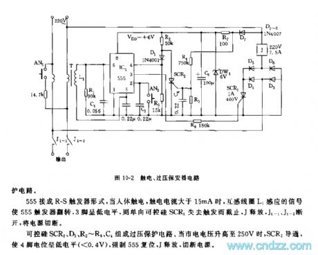
As shown on the figure 10-2, the security monitor includes a reduction voltage rectification circuit,a current transformer, a triggering circuit and a overvoltage protection circuit. The 555 is connected as the R-S trigger,when the body gets an electric shock and the current is greater than 15mA, the L1's actuated signal will make the 555 trigger flip and the three foot turns into the low power level. Then the SCR1 will not touch off, the J will release, the J1-1 and J1-2 will be disconnected, the power will be cut out through this way. The SCR2, D1, R2~R6, C4 make up the overvoltage protection circuit. When the voltage rises to 250V, the SCR2 will be turn-on,then the four foot will be low power level, the 555 will be forcibly reset and the J will be release, the power will be disconnected.
(View)
View full Circuit Diagram | Comments | Reading(1451)
Positive converter circuit diagram composed of TDA4718
Published:2011/7/24 21:28:00 Author:Ecco | Keyword: Positive converter

The positive converter circuit composed of TDA4718 is shown as the chart, and it can convert 220V AC voltage to 5V/10A DC output circuit. In the circuit, the tertiary winding N3, which has the same turns with the primary winding N1, can degauss the core of the transformer during VT1 deadline period, and it charges for filter capacitor C3 by the high-speed diode VD3 in order to improve the conversion efficiency. Self-resonant frequency is determined by the RT and CT. According to component parameters in the diagram, the oscillation frequency is 50kHZ.
(View)
View full Circuit Diagram | Comments | Reading(2301)
MC141628 digital comb filter integrated circuit diagram
Published:2011/7/24 21:18:00 Author:Ecco | Keyword: digital comb filter


MC141628 is the digital comb filter IC produced by Motorola in America, and it is used in a wide range of domestic and imported large screen color TV, such as TCL Kleinwort series of TV and so on. MC141628 integrated circuit includes the voltage-controlled oscillator, digital-analog conversion, standard control switch, digital interface, chromaticity signal processing, clock input mode selection circuit. The lC uses 32-pin dual in-line package, and its data pin functions are listed in Table.
(View)
View full Circuit Diagram | Comments | Reading(450)
The Gate Driving Circuit Composed of TLP559
Published:2011/7/18 5:31:00 Author:nelly | Keyword: Gate Drive Circuit

The picture is the gate driving circuit which applies the TLP559. The TLP559 output circuit is the open collector type, and VT1 does level reverse, thus the output impedance can be reduced in the complementary push-pull circuit. In order to shorten the time of open and off, the capacitor C1 which is parallel with R fastens the capacity. The value of C1 becomes large, and the admittance time becomes short, but the time of open and off becomes longer. Here,C1 selects the 4700pF. The time of open and off will be short even not connected with C1. (View)
View full Circuit Diagram | Comments | Reading(1681)
Gate Driving Half-Bridge Circuit
Published:2011/7/18 5:33:00 Author:nelly | Keyword: Gate Driving, Half-Bridge

In the half-bridge circuit, the gate driving circuit can solve the below problems: the upper arm(high voltage end which is short for high end) drive need isolation; high end driving voltage always needs the voltage which is higher than power supply +UDD, namely UDD+SGS; However, it always uses the bootstrap circuit; the power MOSFET of upper and down arm can not be conducted at the same time, and the time should be predetermined. There are only two power MOSFETsin series with power supply, therefore, the diodes VD1 and VD2 are added, thus the withstand voltage of power MOSFET can close to the power supply. (View)
View full Circuit Diagram | Comments | Reading(468)
Two-way output voltage circuit diagram using MAX668
Published:2011/7/24 21:10:00 Author:Ecco | Keyword: Two-way output voltage

Two-way output voltage circuit using MAX668 is shown as the chart. It can convert +12 V input voltage to 72V/100mA or -24V/400mA output. The circuit is mainly composed of the MAX668 boost converter and MAX4130 op amp and transformer T1. MAX668 is the step-up controller; MAX4130 is the adder, which is used for the feedback of the two-way output voltage; the turns ratio of transformer T1 is set to 1:2:4. When the input voltage changes ± 10%, while the load changes from zero to full load, the circuit allows the two-way output voltage regulation in ± 5%.
(View)
View full Circuit Diagram | Comments | Reading(778)
| Pages:1475/2234 At 2014611462146314641465146614671468146914701471147214731474147514761477147814791480Under 20 |
Circuit Categories
power supply circuit
Amplifier Circuit
Basic Circuit
LED and Light Circuit
Sensor Circuit
Signal Processing
Electrical Equipment Circuit
Control Circuit
Remote Control Circuit
A/D-D/A Converter Circuit
Audio Circuit
Measuring and Test Circuit
Communication Circuit
Computer-Related Circuit
555 Circuit
Automotive Circuit
Repairing Circuit