
Circuit Diagram
Index 1108
STABILIZING_PHOTOMULTIPLIER_GAIN
Published:2009/7/23 23:07:00 Author:Jessie
Feed-back loop provides automatic gain stabilization for color film scanner.-R. M. Farber and K. M. St. John, Scanner Analyzes Color Content of Movie Film, Electronics, 34:48, p 38-41. (View)
View full Circuit Diagram | Comments | Reading(643)
PREFERRED_LOW_LEVEL_AMPLIFIER
Published:2009/7/23 23:06:00 Author:Jessie
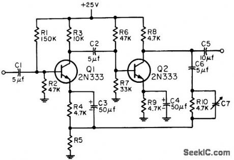
Serves as high-gain amplifier providing stable gain over wide temperature range, with maximum output of 2 v. Is noninverting, has input impedance of 20,000 ohms, and will operate into loads above 10,000 ohms. Several circuits may be cascaded. 2N333 has been dropped front Preferred list, but 2N335 can be used if operating point is adjusted for its larger beta. Voltage gains of 45, 20, or 10 ore obtained for R5 = 100, 220, and 470 ohms respectively.-NBS, Handbook Preferred Circuits Navy Aeronautical Electronic Equipment, Vol. II, Semiconductor Device Circuits, PSC 18 (originally PC 201), p 18-2. (View)
View full Circuit Diagram | Comments | Reading(651)
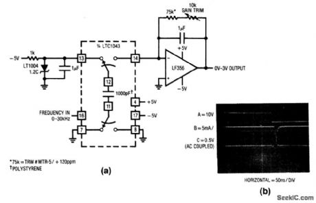
Charge_pump_V_F_converter
Published:2009/7/23 23:06:00 Author:Jessie
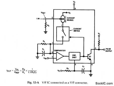
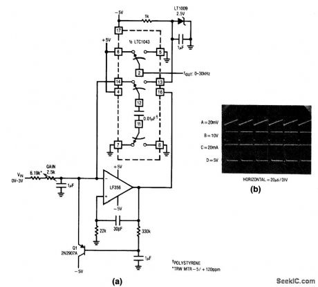
Fig. 12-2 In this circuit, the voltage input is applied to the noninverting input of the LF356, and the LTC1043 is connected in the LF356 feedback loop. This results in a V/F where the oscillation frequency is directly related to input voltage with a transfer linearity of 0.005%. To trim, apply 3.0 V, and adjust gain trim for a 30-kHz Output. Linear Technology, Linear Applications Handbook , 1990 p. AN3-11. (View)
View full Circuit Diagram | Comments | Reading(737)
Linear_current_regulator
Published:2009/7/23 23:06:00 Author:Jessie
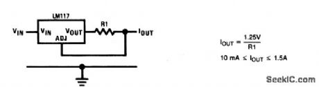
This circuit provides regulated current from 10mA to 1.5A, depending on the value of R1. (View)
View full Circuit Diagram | Comments | Reading(662)
WIDEBAND_VIDEO_AMPLIFIER
Published:2009/7/23 23:06:00 Author:Jessie
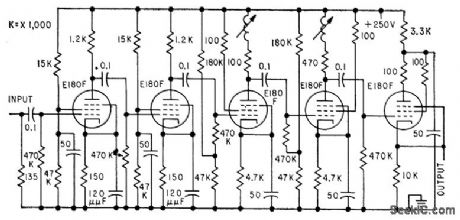
Has gain of 1,000, bringing 1-mV input up to 1 V. First two stages are cathode-bypassed, and next two use inductive compensation for high-frequency peaking, to compensate for non infinitesimal short persistence of screen of flying-spot scanner. Used in comparing two sky photographs to detect variable stets.-J. Borgman, Using Tv Techniques in Astron. omy, Electronics, 32:19, p 66-68. (View)
View full Circuit Diagram | Comments | Reading(517)
SILICON_WIDEBAND_VIDEO_AMPLIFIER
Published:2009/7/23 23:05:00 Author:Jessie
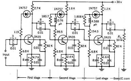
Employs feedback around each of its three stages, with zener diode for stabilizing collector. emitter voltage. Voltage and current amplification are 20 db, and useful frequency range is 3.2 kc to 32 Mc,-Texas Instruments Inc., Transistor Circuit Design, McGraw-Hill, N.Y., 1963, p 267. (View)
View full Circuit Diagram | Comments | Reading(748)
Positive_and_negative_voltage_converter
Published:2009/7/23 23:05:00 Author:Jessie
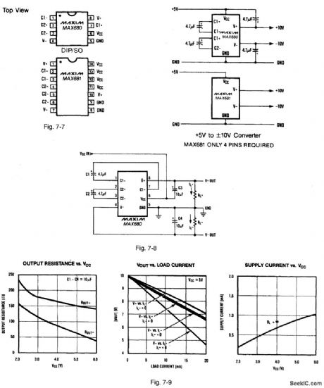
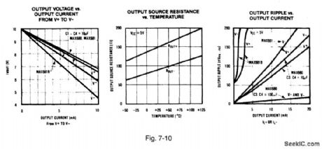
Figure 7-7 shows MAX680 and MAX681 converters used to provide ±10-V outputs from a +5-V input. The input voltage range is +2.0 V to +6.0 V. Voltage-conversion efficiency is 95%, with 85% power-conversion efficiency. The supply current is 500 μA. The output source impedances are typically 150 Ω, providing useful output currents up to 10 mA. No extemal capacitors are required for the MAX681. Figure 7-8 shows a test circuit. Figures 7-9 and 7-10 show typical test results. MAxIM NEw RELEASES DATA BOOK, 1992, P. 4-141. (View)
View full Circuit Diagram | Comments | Reading(719)
Linear_regulator_with_multiple_outputs
Published:2009/7/23 23:05:00 Author:Jessie
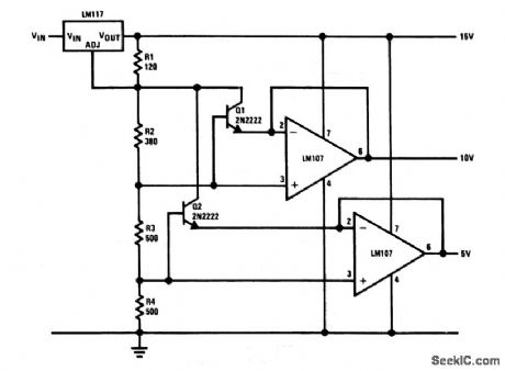
This circuit provides +5-, +10-, and +15-V regulated outputs. (View)
View full Circuit Diagram | Comments | Reading(524)
SHAPE_RECOGNITION
Published:2009/7/23 23:05:00 Author:Jessie
Use of dilating circular scan resolves some of problems for general-purpose reading machine. Technique can be applied to automatic recognition of letters and numbers in variety of styles.-L. D. Harmon, Line-Drawing Pattern Recognizer, Electronics, 33:36, p 39-43. (View)
View full Circuit Diagram | Comments | Reading(686)
Linear_voltage_regulator_and_voltage_reference
Published:2009/7/23 23:04:00 Author:Jessie

This circuit provides a +15-V regulated output, as well as a 6.95-V voltage reference. (View)
View full Circuit Diagram | Comments | Reading(566)
CASCADED_SHUNT_PEAKED_STAGES
Published:2009/7/23 23:04:00 Author:Jessie
Design procedure is given for n identical one-pole stages. Bandwidth of total cascaded amplifier is equal to bandwidth of single stage multiplied by shrinkage factor of 0.64 for two stages, 0.51 for three, and 0.44 for four. two stage example shown gives gain of 8.5 and bandwidth of 2.1 Mc.-R. S. Pepper and D. O. Pederson, Designing Shunt-Peaked Transistor Amplifiers, Electronics.33:49, p 68-70. (View)
View full Circuit Diagram | Comments | Reading(1475)
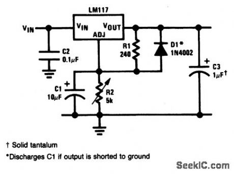
Adjustable_regulator_with_protective_diodes
Published:2009/7/23 23:10:00 Author:Jessie
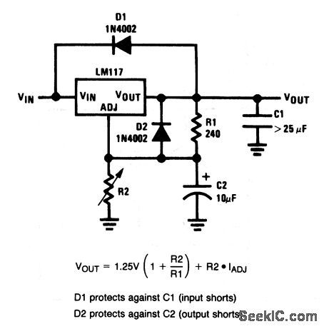
This circuit is similar to that of Fig. 7-11, but with diodes that protect against capacitor discharge (because of input or output shorts). (View)
View full Circuit Diagram | Comments | Reading(625)
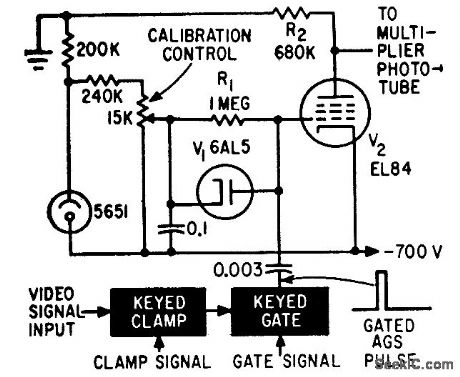
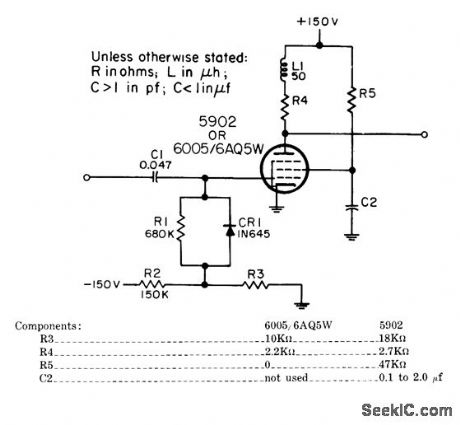
FLYING_SPOT_SCANNER_PROTECTS_MICRO_FILM
Published:2009/7/23 23:10:00 Author:Jessie
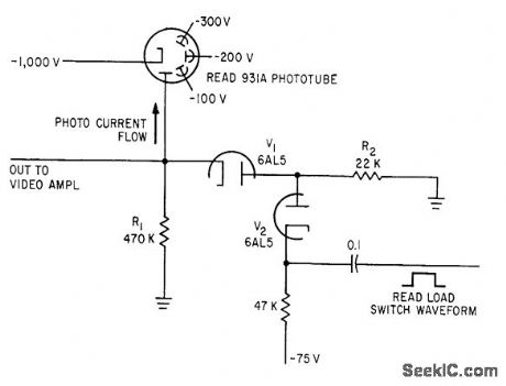
When black mark on microfilm covers quiescent spot, sweep is tripped and rectangular pulse on cathode of V2 cuts it off. 931A multiplier phototube then sees 22,000-ohm load through V1 to give correct output.-A. C. L. Brown, Flying Spot Inspects Tv Rating Records, Electronics, 35;9, p 31-34. (View)
View full Circuit Diagram | Comments | Reading(632)
PREFERRED_VIDEO_AMPLIFIER_CHAIN
Published:2009/7/23 23:10:00 Author:Jessie
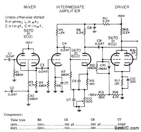
Designed for use in radar display system to mix positive radar video with positive marker pulses, to invert combined signals, and to amplify them sufficiently to intensity-modulate cathode-ray indicator. Input polarity is negative. Maximum peak amplitude is 60 v. Amplification is variable from 30 to 60.-NBS, Handbook Preferred Circuits Navy Aeronautical Electronic Equipment, Vol. I, Electron tube Circuits, 1963, PC 25, p 25-2. (View)
View full Circuit Diagram | Comments | Reading(686)
FLAT_TUBE_SCANNER
Published:2009/7/23 23:09:00 Author:Jessie
V1 thru V3 generate sawtooth wave and V5 thru V7 triangular wave for driving horizontal and vertical conductors of electroluminescent panel. -B. Binggeli and E. Fatuzzo, Solid-State Panels: Will They Bring Flat-Display TV? Electronics, 35:26, p 67-70. (View)
View full Circuit Diagram | Comments | Reading(772)
Adjustable_regulator_with_improved_ripple_rejection
Published:2009/7/23 23:09:00 Author:Jessie
This circuit is similar to that of Fig. 7-11, but with improved ripple rejection. (View)
View full Circuit Diagram | Comments | Reading(626)
Charge_pump_F_V_converter
Published:2009/7/23 23:09:00 Author:Jessie
Pig. 12-1 In this circuit, the frequency input is applied to the clock input of an LTC1043 switched-capacitor IC. The 1000-pF capacitor is switched between a fixed voltage and the inverting input of the LF356. The 1-pF feedback capacitor averages this action over several cycles, and the circuit output is a dc level that is linearly related to frequency. The feedback resistors set the LF356 gain. Note that the input pulse width must be low for at least 100 ns to allow complete discharge of the 1000-pF capacitor. To trim, apply 30-kHz to pin 16 of the LTC1043 and set the gain trim for exactly 3.0V. Linear Technology Linear Applications Handbook 1990p.AN3-11. (View)
View full Circuit Diagram | Comments | Reading(609)
Two_wire_current_transmitter
Published:2009/7/23 23:09:00 Author:Jessie
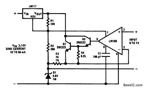
This circuit has a 10- to 50-mA output for a 1-V input. The minimum operating voltage is about 12 V. The circuit can be used in 4- to 20-mA current-transmitter applications (industrial control). However, the LM117 should be selected for low quiescent current. (View)
View full Circuit Diagram | Comments | Reading(593)
PREFERRED_BEAM_POWER_DRIVER
Published:2009/7/23 23:08:00 Author:Jessie
Used in search radars to amplify video signals to 60.v level required for intemsity modulation of cathode-ray indicator. Input polarity is positive. Amplification is 7.-NBS, Hand-book Preferred Circuits Navy Aeronautical Electronic Equipment, Vol. I, Electron Tube Circuits, 1963, PC 28, p 28-2.
(View)
View full Circuit Diagram | Comments | Reading(616)
30_W_150__to_175_MHz_amplifier
Published:2009/7/23 23:08:00 Author:Jessie
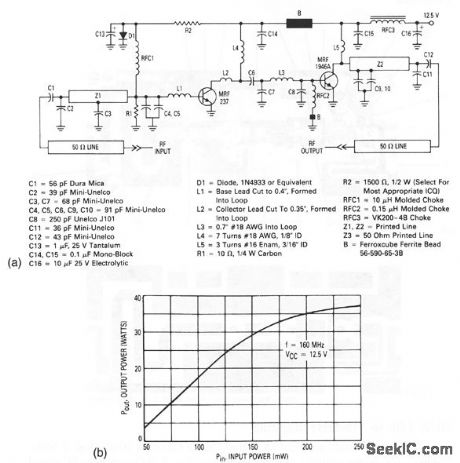

This circuit produces an overall gain in excess of20 dB (Fig. 2-56B).Figure 2-56C shows typical parts placement, and Fig. 2-56D shows the PC-board photomaster (actual dimensions: 5 x 2 ). The amplifier is constructed on 1/16 , double-sided G-10 board with 2-ounce copper cladding. The top and bottom ground planes of the board are connected by wrapping the board edges with thin copper foil (0.002 ) and then soldering the foil in place. The MRF237 is inserted into a hole in the board and soldered to the ground plane for heatsinking. The MRF1946A is mounted on a conventional heatsink (an 8-32 stud inserted into an appropriately prepared heatsink). Refer to Motorola AN778 and AN790 for mounting and thermal ratings of power transistors.
(View)
View full Circuit Diagram | Comments | Reading(1925)
| Pages:1108/2234 At 2011011102110311041105110611071108110911101111111211131114111511161117111811191120Under 20 |
Circuit Categories
power supply circuit
Amplifier Circuit
Basic Circuit
LED and Light Circuit
Sensor Circuit
Signal Processing
Electrical Equipment Circuit
Control Circuit
Remote Control Circuit
A/D-D/A Converter Circuit
Audio Circuit
Measuring and Test Circuit
Communication Circuit
Computer-Related Circuit
555 Circuit
Automotive Circuit
Repairing Circuit