
Circuit Diagram
Index 1115
CLAMP_ON_CURRENT_PROBE_COMPENSATOR
Published:2009/7/3 4:04:00 Author:May
Circuit Notes
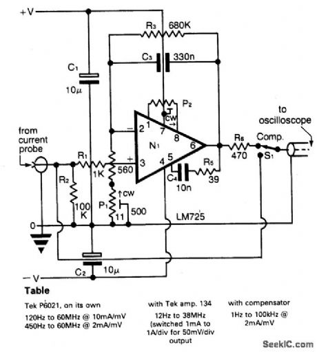
A clamp-on“current probe such as the Tektronix P6021 is a useful means of displaying current waveforms on an oscilloscope. Unfortunately, the low-frequency response is somewhat limited, as shown in the Table.The more sensitive range on the P6021 is 2 mA/mV, but it has a roll-off of 6 dB per octave below 450 Hz. The compensator counteracts the low-frequency attenuation, and this is achieved by means of C3 and R4 + P1 in the feedback around op amp N1.The latter is a low-noise type, such as the LM725 shown, and even so it is necessary at some point to limit the increasing gain with decreasing frequency; otherwise amplifier noise and drift will overcome the signal. The values shown for C3R3 give a lower limit below 1 Hz. A test square wave of ±10mA is fed to the current probe so that P1 can be adjusted for minimum droop or overshoot in the output waveform. At high frequencies, the response begins to fall off at 100 kHz. (View)
View full Circuit Diagram | Comments | Reading(1524)
BATTERY_CHARGER
Published:2009/7/3 4:03:00 Author:May
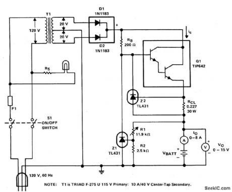
The charger is based on a charging voltage of 2.4 V per cell, in accordance with most manufacturers' recommendations. The circuit pulses the battery under charge with 14.4 V (6 cells × 2.4 V per cell) at a rate of 120 Hz. The design provides current limiting to protect the charger's internal components while limiting the charging rate to prevent damaging severely discharged lead-acid batteries. The maximum recommended charging current is normally about one-fourth the ampere-hour rating of the battery. For example, the maximum charging current for art average 44 ampere-hour battery is11 A. If the impedance of the load requires a charging current greater than the 11 A current limit, the circuit will go into current limiting. The amplitude of the charging pulses is controlled to maintain a maximum peak charging current of 11 A (8 A average). (View)
View full Circuit Diagram | Comments | Reading(3803)
Ni_CAD_BATTERY_ZAPPER_II
Published:2009/7/3 4:01:00 Author:May
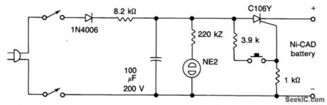
This zapper clears intemal short in nickel cadmium batteries by buming it away. CAUTION: The negative battery terminal is connected to one side of the ac line. For safety operation use a 1:1 isolation transformer. (View)
View full Circuit Diagram | Comments | Reading(863)
LEVEL_SHIFT_WITH_IC
Published:2009/7/3 4:00:00 Author:May
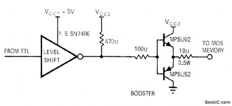
Level shifter for dynamic MOS random-access memory uses SN7406 IC with two-transistor booster to convert TTL levels to MOS levels. Booster can be omitted for data input lines because they drive such low capacitive loads in typical arrays.-M.E. Hoff, Designing an LSI Memory System That Outperforms Cores-Economically, Computer Hardware (section of EDN Magazine), Jan. 15, 1971, p 6-15 (p 000110-001111). (View)
View full Circuit Diagram | Comments | Reading(1819)
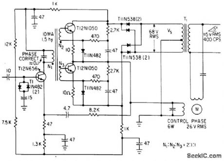
50_60_and_400_CPS_SERVO_AMPLIFIER
Published:2009/7/23 23:51:00 Author:Jessie
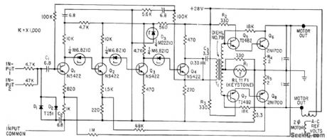
Solid-state 10-W amplifier handles all three power frequencies, operates from 28 V d-c, and uses four-transistor Darlington output stages to drive two-phase servo motor. Preamplifier and drive stages Q1-Q4 are all d-c coupled through zener diodes, with d-c feedback around all four stages to stabilize bias against temperature changes.-M. Bodnar, Versatile Servo Amplifier for 50, 60 or 400-Cycle Operation, Electronics, 36:3, p 44-45. (View)
View full Circuit Diagram | Comments | Reading(1499)
THERMALLY_CONTROLLED_Ni_CAD_CHARGER
Published:2009/7/3 4:00:00 Author:May
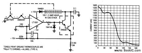
One way to charge Ni-Cad batteries rapidly without abuse is to measure cell temperature and taper the charge accordingly. The circuit uses a thermocouple for this function. A second thermocouple nulls out the effects of ambient temperature. The temperature difference between the two thermocouples determines the voltage which appears at the amplifier's positive input. As battery temperature rises, this small negative voltage (1℃ difference between the thermocouples equals 40 μV) becomes larger. The amplifier, operating at a gain of 4300, gradually reduces the current through the battery to maintain its inputs at balance. The battery charges at a high rate until heating occurs and the circuit then tapers the charge. The values given in the circuit limit the battery surface temperature rise over ambient to about 5℃. (View)
View full Circuit Diagram | Comments | Reading(493)
LITHIUM_BATTERY_CHARGER
Published:2009/7/3 3:59:00 Author:May
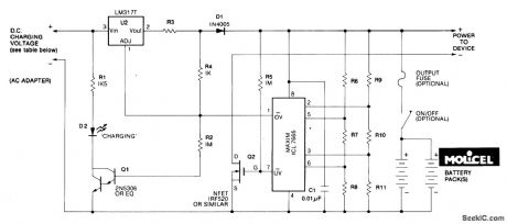
Charging is accomplished with a constant current of 60 mA for AA cells to a cutoff voltage of 2.4 V per cell at which point the charge must be terminated. The charging system shown is designed for multi-cell battery packs of 2 to 6 series-connected cells or series/parallel arrangements. It is essential that all cells assembled in the pack be at an identical state-of-charge (voltage) prior to charging. The maximum upper cut-off voltage is 15.6 volts (6 x 2.6 V). (View)
View full Circuit Diagram | Comments | Reading(2107)
Single_cell_V_F_converter__25_Hz_to_10_kHz
Published:2009/7/23 23:51:00 Author:Jessie
Fig. 12-1 7 This circuit is similar to that of Fig. 12-11, except that a 0- to 1-V input produces a 25-Hz to 10-kHz output. Transfer linearity is 0.25%, drift is 250 ppm/℃, and current consumption is about 205μA (compared to the 125-μA drain in the Fig. 12-11 circuit). To trim, first select the 100-kΩ resistor so that VCLAMP (Q2 emitter) is at 1 V. Next, apply 2.5 mV at the input and select the resistor value indicated at the C1 input for 25-Hz output. Then, apply exactly 1 V and adjust the 10-kHz trim for a 10-kHz output. Linear Technology Linear Applications Handbook 1990, p AN15-1. (View)
View full Circuit Diagram | Comments | Reading(663)
Ni_CAD_BATTERY_ZAPPER
Published:2009/7/3 3:57:00 Author:May
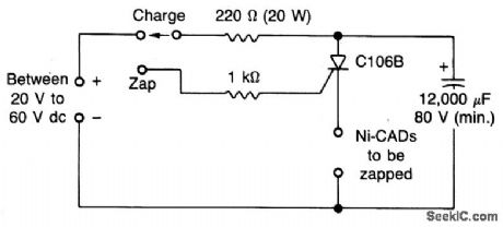
The short in a Ni-Cad battery can be burned off with this zapper. Use of the SCR keeps heavy discharge current from damaging switch contacts. (View)
View full Circuit Diagram | Comments | Reading(663)
GEL_CELL_CHARGER
Published:2009/7/3 3:56:00 Author:May
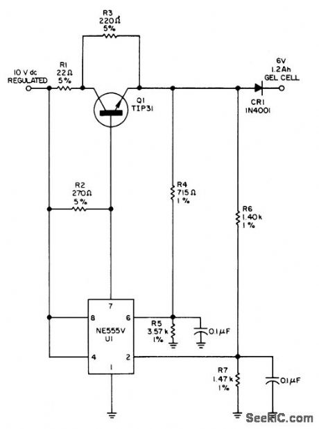
This circuit detects a full-charge state andautomatically switches to a float condition-from240 mA to 12 mA. (View)
View full Circuit Diagram | Comments | Reading(533)
5_A_positive_fixed_current_regulator
Published:2009/7/23 23:50:00 Author:Jessie
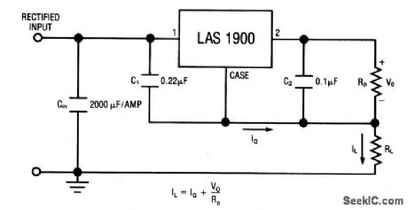
This circuit uses the LAS1900 series voltage regulator (Fig. 7-46) as a fixed-current regulator. Characteristics are shown in Fig. 7-46B, 7-46C, and 7-46D. (View)
View full Circuit Diagram | Comments | Reading(599)
HEART_MONITOR
Published:2009/7/3 3:55:00 Author:May
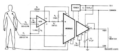
Electrocardiograph amplifier uses Burr-Brown BB3656 isolation amplifier to protect electrocardiograph from inadvertent applications of defibrillation pulses while patient is being monitored. Heart pulses are accurately amplified over frequency range of DC to 3 kHz. Resistors must be carbon-composition types.-B.Olschewski, Unique Transformer Design Shrinks Hybrid Isolation Amplifier's Sizeand Cost.Electronics.July 20.1978.p105-112. (View)
View full Circuit Diagram | Comments | Reading(3903)
6_WAlT_SERVO_AMPLIFIER
Published:2009/7/23 23:50:00 Author:Jessie
Unconventional output stage eliminates need for center tap on servomotor for controlled winding, gives 55% overall efficiency.-J. A. Walston and J. E. Setliff, Designing Servo Amplifiers for High Efficiency, Electronics, 36;6, p 62-63. (View)
View full Circuit Diagram | Comments | Reading(620)
RAPID_BATTERY_CHARGER_FOR_ICOM_IC_2A
Published:2009/7/3 3:55:00 Author:May

Rectifted and filtered voltage from the 24 Vac transformer is applied to the LM723 voltage regulator and the npn pass transistor set up for constant current supply. The 470 ohm resistor limits trickle current until the momentary pushbutton (S2) is depressed, the SCR turns on and current ftows through the previously determined resistor network limiting the charging current. The SCR will turn off when the thennal cutout circuit inside the battery pack opens up. (View)
View full Circuit Diagram | Comments | Reading(2846)
ACTIVE_CLAMP_LIMITING_AMPLIFIER
Published:2009/7/3 3:52:00 Author:May

The modified inverting amplifier uses an active clamp to limit the output swing with precision.Allowance must be made for the VBEof the transistors. The swing is limited by the base- emitter breakdown of the transistors. A simple circuit uses two back-to-back zener diodes across the feedback resistor, but tends to give less precise limiting and cannot be easily controlled. (View)
View full Circuit Diagram | Comments | Reading(868)
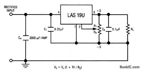
5_A_positive_adjustable_voltage_regulator
Published:2009/7/23 23:50:00 Author:Jessie
The LAS19U is a four-terminal adjustable regulator IC with an output range from +4 to +30V, providing remote sensing from a single pot. Characteristics are shown in Fig. 7-46B, 7-46C, and 7-46D. (View)
View full Circuit Diagram | Comments | Reading(749)
5_A_positive_fixed_voltage_regulator
Published:2009/7/23 23:49:00 Author:Jessie
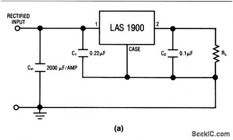
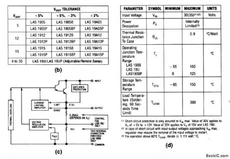
The LAS1900 series voltage regulators are ICs containing all elements necessary for linear regulation (safe area protection, thermal overload, current limiting, as shown in Fig. 7-46C). Figure 7-46B shows the output voltage and tolerance for the various LAS1900 part numbers. Figure 7-46D shows the absolute maximum ratings. (View)
View full Circuit Diagram | Comments | Reading(742)
AUDIBLE_TUNING_FOR_BLIND
Published:2009/7/3 3:51:00 Author:May
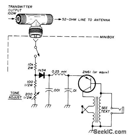
Transmitter or exciter output is sampled at coax line and highresistance voltage divider. Rectified voltage of divider, which varies during transmitter tuning, is fed to relaxation oscillator whose output varies in pitch with voltage; low voltage gives high-pitched tone, and high voltage gives lowpitched tone. Input divider draws about 1 W from 100-W transmitter; for higher power, such as 1 kW, change 10K to about 100K. Diode feeds about 2 V to emitter of transistor. Any audiotype PNP transistor can be used. For NPN device, reverse diode connections. Transformer is from 5-W transistor amplifier, with 22-ohm high-impedance winding. Other two windings, in series aiding, are 4 ohms each.-D.H. Atkins, Tuning Aid for the Sightless, Ham Radio, Sept.1976, p 83 (View)
View full Circuit Diagram | Comments | Reading(561)
Line_isolation
Published:2009/7/23 23:48:00 Author:Jessie
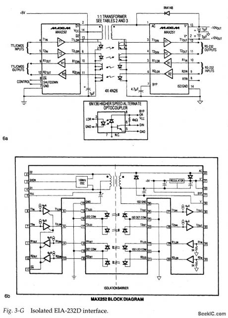
In telecom systems, the service provider incorporates line isolation to protect the network against unorthodox connections made by users. At the other end of the line, EIA-232D connections used in medical patient-monitoring equipment, data loggers, and supervisory computers (to name a few devices) must be isolated to protect the equipment from hardware failures. Isolation not only provides safety, but it can improve system performance.
As an example, EIA-232D links between a computer in one building and terminals in another building can show ground-current noise if the building earth-ground connections are at different potentials (as is usually the case). Isolation with a rating of 100 V can solve this problem. In severe industrial environments, a full UL-listed isolation barrier of 1500 V (or more) might be required.
The transmission of digital data, while maintaining an electrical barrier, usually involves transformers and opto-isolators, as shown in 6a of Fig. 3-G. The transformer supplies power to the other side of the barrier, and the opto-couplers handle data transmission across the barrier. However, there is a problem with this approach. The LEDs in opto-isolators (especially high-speed opto-isolators) require more current than normal logic circuits can provide. As a result, you must connect the outputs in parallel or add buffer ICs to get adequate drive current. Also, the isolated power supply must be fairly large because standard EIA-232D chips require a supply voltage of ±12V, as well as +5 V.
One approach to solving these power and data-transfer problems is to use matching interface chip sets, such as the MAX250/MAX251, shown in 6a of Fig. 3-G. These two ICs include circuitry for two EIA-232D transmitters and two receivers, circuitry for generating isolated power-supply voltage from the main (non-isolated) +5-V supply, and interface circuitry for driving and receiving signals from the external opto-isolators. You only need to supply the isolators, a 1:1 transformer, and a few passive components to complete an isolated dual-transceiver EIA-232D port. (Such circuits are covered in this chapter)
The alternate approach is to use a single-chip interface, such as the MAX252 shown in 6b of Fig. 3-G. This IC includes all of the circuitry in a standard 40-pin DIP, but provides the full UL-recognized 1500-V isolation barrier. (This approach is also covered in this chapter.) (View)
View full Circuit Diagram | Comments | Reading(1127)
DIFFERENTIAL_AMPLIFIER
Published:2009/7/3 3:50:00 Author:May
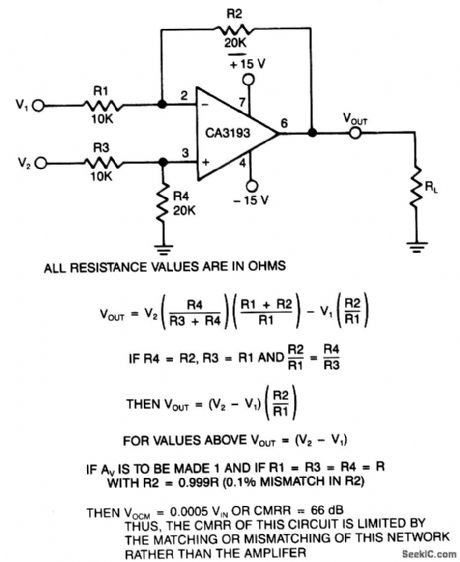
This differential amplifier uses a CA3193 BiMOS op amp. This classical, differential input-to-signal-ended output converter when used with lowresistance signal source will maintain level of CMRR, if R1=R3 + R4. (View)
View full Circuit Diagram | Comments | Reading(4708)
| Pages:1115/2234 At 2011011102110311041105110611071108110911101111111211131114111511161117111811191120Under 20 |
Circuit Categories
power supply circuit
Amplifier Circuit
Basic Circuit
LED and Light Circuit
Sensor Circuit
Signal Processing
Electrical Equipment Circuit
Control Circuit
Remote Control Circuit
A/D-D/A Converter Circuit
Audio Circuit
Measuring and Test Circuit
Communication Circuit
Computer-Related Circuit
555 Circuit
Automotive Circuit
Repairing Circuit