
Circuit Diagram
Index 1113
FOUR_INPUT_VIDEO_MIXER
Published:2009/7/23 23:29:00 Author:Jessie
Used for combining four different positive-polarity marker pulses in radar system.-NBS, Handbook Preferred Circuits Navy Aeronautical Electronic Equipment, Vol. 1, Electron Tube Circuits, 1963, p N4-1. (View)
View full Circuit Diagram | Comments | Reading(598)
15_A_positive_fixed_voltage_regulator
Published:2009/7/23 23:28:00 Author:Jessie


The LAS1500 series voltage regulators are ICs that contain all elements necessary for linear regulation (safe-area protection, thermal overload, and current limiting, as shown in Fig. 7-32C). Figure 7-32B shows the output voltage and tolerance for the various LAS1500 part numbers. Figure 7-32D shows the absolute maxirnum ratings. (View)
View full Circuit Diagram | Comments | Reading(590)
FIVE_INPUT_VIDEO_MIXER
Published:2009/7/23 23:28:00 Author:Jessie

Combines five radar marker inputs.-NBS, Handbook Preferred Circuits Navy Aeronautical Electronic Equipment, Vol. 1, Electron Tube Circuits, 1963, p N4-2. (View)
View full Circuit Diagram | Comments | Reading(802)
TRANSDUCER_SCANNER
Published:2009/7/23 23:28:00 Author:Jessie
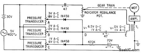
Monitors transducer outputs in parallel mode and reports when any one of measured parameters exceeds or falls below predetermined limit. Superimposing ac signal on d-c control voltage permits use of a-c servo as indicator.-S. Thaler, Solid. State Parallel-Mode Stunner Reads System Physical Parameters, Electronics, 34:19, p 78-80. (View)
View full Circuit Diagram | Comments | Reading(626)
Low_cost_two_chip_AM_radio_system
Published:2009/7/23 23:28:00 Author:Jessie


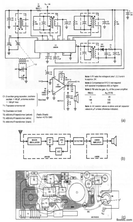
This AM radio requires only two ICs and few discrete components. A block diagram of the radio is shown in Fig. 2-63B. The typical PC-board layout is shown in Fig. 2-63C. The mixer-oscillator, two IF stages, and AGC section are contained within the LM3820. The power output of 0.25-W into an 8-Ω speaker is obtained in the LM386. (View)
View full Circuit Diagram | Comments | Reading(1369)
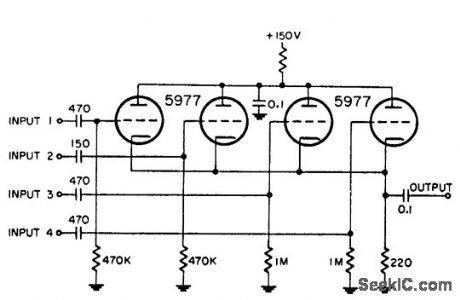
FOUR_TRIGGER_VIDEO_MIXER
Published:2009/7/23 23:27:00 Author:Jessie

Common-cathode arrangement with 47K cathode resistor allows nonadditive mixing of four positive trigger pulses having amplitudes in vicinity of 50 v.-NBS, Handbook Preferred Circuits Navy Aeronautical Electronic Equipment, Vol. 1, Electron lube Circuits, 1963, p N4-1. (View)
View full Circuit Diagram | Comments | Reading(822)
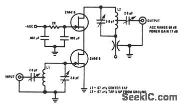
High_current_amplifier_with_rail_to_rail_output
Published:2009/7/23 23:27:00 Author:Jessie

This circuit features rail-to-rail output swing, but with currents higher than with the circuits of Figs. 1-10 and 1-11. Bandwidth is 600 kHz, and slew rate exceeds 24 V/μs under 100-mA output loading. (View)
View full Circuit Diagram | Comments | Reading(793)
8_A_positive_fixed_voltage_regulator
Published:2009/7/23 23:52:00 Author:Jessie

The LAS3905 series voltage regulators are ICs that contain all elements necessary for linear regulation (safe-area protection, thermal overload, and current limiting, as shown in Fig. 7-50C). Figure 7-50B shows the output voltage and tolerance for the various LAS3905 part numbers. Figure 7-50D shows the absolute maximum ratings. (View)
View full Circuit Diagram | Comments | Reading(721)
Low_noise_dc_stabilized_amplifier
Published:2009/7/23 23:52:00 Author:Jessie


This circuit combines a low-drift chopper-stabilized amplifier with an ultra-low noise bipolar amplifier. The LTC1052 measures the dc error at the LT1028 input terminals, and biases the offset pins to force offset to a few microvolts. As a result, noise is kept to a minimum. The combined characteristics of these amplifiers yield the following: offset voltage = 5μV max. offset drift = 50 nV/℃, and noise 1.1 nV HZ. Figure 1-23B plots noise amplitude over time in a 0.1- to 10-Hz bandwidth. . (View)
View full Circuit Diagram | Comments | Reading(839)
BATTERY_STATUS_INDICATOR
Published:2009/7/3 4:22:00 Author:May

Continually monitors battery voltage during use and consumes only about 250 pA (until the end point is reached). Near the end point Tr1 turns off, allowing Tr2 to illuminate the LED to increase current drain further leading to a distinct turn off point. (View)
View full Circuit Diagram | Comments | Reading(1855)
VOLTAGE_DETECTOR_RELAY_FOR_BATTERY_CHARGER
Published:2009/7/3 4:21:00 Author:May

While the battery is being charged, its voltage is measured at V. If the measured voltage is lower than the minimum the relay will be energized, that will connect the charger circuit. When the battery voltage runs over the maximum set point, the relay is deenergized and it will be held that way until the voltage decreases below the minimum when it will be connected again. The voltage is lower than a threshold VB (low breaking voltage) the relay will be assumed that such a low voltage is due to one or several dam-aged battery components. Of course VB is much lower than the minimum set point. (View)
View full Circuit Diagram | Comments | Reading(883)
DIRECT_COUPLED_PREAMP
Published:2009/7/23 23:52:00 Author:Jessie
Direct-coupled silicon-transistor ampli0et uses zener diode to provide constant voltage, and has adequate d-c stability even with transistors having beta range of 3:1.-A. N. Desautels, Servo Preamplifiers Using Direct-Coupled Transistors, Electronics, 32:20, p 74. (View)
View full Circuit Diagram | Comments | Reading(0)
GARRIER_SYSTEM_RECEIVER_
Published:2009/7/3 4:21:00 Author:May

Used to detect,amplify,limit,and demodulate FM carrier modulated with audio ρrogram、for feeding up to 2.5 W to remote loudspeaker. Can be plugged into any AC outlet on same side of distribution transtormer. Carrier signal is taken lrom line by tuned transtormerr,. Output of two-stage Iimiter amplifier Q1A-Q1D is applied directlv to mute peak detector D1-Q2-C7. Limiter output is reduced to1 V P-P for driving National LM565CN PLL detector which operates as narrow-band tracking filter for input signal and provides low-distortion demodulated audio output. Mute circuit quiets receiver in absence of carrier.-J. Sherwin, N. Sevastopoulos, and T, Regan, FM Remote Speaker System, National Semiconductor, Santa Clara, CA, 1975, AN-146. (View)
View full Circuit Diagram | Comments | Reading(835)
DYNAMIC,CONSTANT_CURRENT_LOAD_FOR_FUEL_CELL_BATTERY_TESTING
Published:2009/7/3 4:20:00 Author:May

This circuit was designed for testing fuel cells, but it could also be used for testing batteries under a constant current load. It provides a dynamic, constant current load, eliminating the need to manually adjust the load to maintain a constant load.
For fuel cell application, the load must be able to absorb 20-40 A, and since a single cell develops only 0.5 to 1.0 V, bipolar power devices (such as a Darlington) are impractical. Therefore, this dynamic load was designed with a TMOS Power FET (Q2).
With switch S1 in position 1, emitter follower Q1 and R1 establish the current level for the load. In position 2, an extemal voltage can be applied to control the current level.
Operational amplifier U1 drives TM0S device Q1, which sets the load current seen by the fuel cell or battery. The voltage drop across R15, which is related to the load current, is then applied to U2, whose output is fed back to U1. Thus, if the voltage across R15 would tend to change, feedback to the minus input of U1 causes that voltage (and the load current) to remain constant. Adjustment of R13 controls the volts/amp of feedback. The VOUT point is used to monitor the system. (View)
View full Circuit Diagram | Comments | Reading(2999)
LATCH_MEMORY
Published:2009/7/3 4:18:00 Author:May
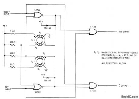
Use of saturable transformers makes memory nonvolatile and immune to false command signals. Transformers stay magnetically biased without voltage supply to provide reference state to which memory latch retumswhen power is reapplied. When bit is initially stored in circuit, set or reset pulse must have minimum width of 35 μs and minimum separation of 65 μs.-G. E. Bloom, Saturable Core Transformers Harden Latch Memories, Electronics, March 31, 1977, p 104-105. (View)
View full Circuit Diagram | Comments | Reading(780)
14_VOLT,4_AMP_BATTERY_CHARGER_POWER_SUPPLY
Published:2009/7/3 4:18:00 Author:May

Operation amplifier A1 directly drives the VN64GA with the error signal to control the output voltage. Peak rectifier D1, C1 supplies error amplifier A1 and the reference zener. This extra drive voltage must exceed its source voltage by several volts for the VN64GA to pass full load current. The output voltage is pulsating dc which is quite satisfactory for battery charging. To convert the system to a regulated dc supply, capacitor C2 is increased and another electrolytic capacitor is added across the load. The response time is very fast, being determined by the op-amp. The 2N4400 current limiter circuit prevents the output current from exceeding 4.5 A. However, maintaining a shorted condition for more than a second will cause the VN64GA to exceed its temperature ratings.A generous heat sink, on the order of 1℃/W, must be used. (View)
View full Circuit Diagram | Comments | Reading(1514)
VERSATILE_BATTERY_CHARGER
Published:2009/7/3 4:15:00 Author:May

An LM317 voltage regulator is configured as a constant-current source. It is used to supply the 50 mA charging current to S01-S06, an array of AA-cell battery holders. Each of the battery holders is wired in series with an LED and its associated shunt resistor. When the battery holder contains a battery, the LED glows during charging. Each battery holder/LED combination is paralleled by a 5.1-volt Zener diode. If the battery holder is empty, the Zener conducts the current around the holder.A timing circuit prevents overcharging. When power is applied to the circuit, timing is initiated by IC2, a CD4541 oscillator/programmable timer. The output of IC2 is fed to Q1. When that output is high, the transistor is on, and the charging circuit is completed.When the output is low, the transistor is off, and the path to ground is interrupted. (View)
View full Circuit Diagram | Comments | Reading(2606)
1_kHz_FIFTH_ORDER_LOW_PASS
Published:2009/7/3 4:15:00 Author:May

Used with 1-kHz signal generator to remove unwanted harmonics,leaving pure sine wave as required formeasuring distortion in modern audio amplifiefs Attenuation peaks are carefuny positionedto coincide with second and third harmonics,giving 65-dB attenuation of these harmonicsand at least 50-dB attenuation of higher hatmonics.-J A,Hardcastle,1 kHz Source Cleaning Filter,Wireless World,Oct,1978,p 59. (View)
View full Circuit Diagram | Comments | Reading(0)
PROM_POWER_DOWN
Published:2009/7/3 4:15:00 Author:May
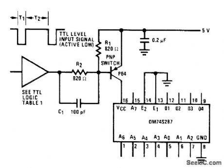
Conserves power in applications when data is required from PROM for only small percentage of system cycle. Circult turns PROM off automatically when not needed, with access time increased only by 80-ns delay of power-down circuit. PNP switch can be PN4313 or 2N3467 pass transistor. With two 74S04 sections in series at input, active low selection is obtained. 74S00 at input gives active high selection. When logic input to R2 goes low, PNP switch is turned on and +5V is applied to National DM74S287 256 x 4 PROM.- Memory Applications Handbook, National Semiconductor, Santa Clara, CA, 1978, p 5-9-5-12. (View)
View full Circuit Diagram | Comments | Reading(816)
Timer_F_V_converter
Published:2009/7/23 23:52:00 Author:Jessie

Fig.12-18 This circuit uses an LM122 timer as a basic F/V converter. The LM122 timer as a basic F/V converter. The LM122 output pulses are averaged with a simple one-pole filter to provide a dc output that is directly related to the trigger input frequency. The pulse width is adjusted with R2 to provide initial calibration at 10kHz. Linearity is about 0.2% for a 0-to 1-V output. A series RC network across the meter provides damping and will improve response at very low frequencies. (View)
View full Circuit Diagram | Comments | Reading(1399)
| Pages:1113/2234 At 2011011102110311041105110611071108110911101111111211131114111511161117111811191120Under 20 |
Circuit Categories
power supply circuit
Amplifier Circuit
Basic Circuit
LED and Light Circuit
Sensor Circuit
Signal Processing
Electrical Equipment Circuit
Control Circuit
Remote Control Circuit
A/D-D/A Converter Circuit
Audio Circuit
Measuring and Test Circuit
Communication Circuit
Computer-Related Circuit
555 Circuit
Automotive Circuit
Repairing Circuit