
Circuit Diagram
Index 1111
High_stability_linear_regulator
Published:2009/7/23 23:19:00 Author:Jessie

The load and line regulation of this circuit is better than 0.001%.Noise, drift, and long-term stability are determined by Zener D1. Noise can be reduced by inserting 100-kΩ resistors in series with both inputs of the LM108A, and bypassing the noninverting input to ground. A 100-pF capacitor between the LM108A output and the inverting input prevents frequency stability. Temperature drift can be reduced by adjusting R4 for minimum drift. For best results, remote sensing should be made directly to the load terminals, as shown. (View)
View full Circuit Diagram | Comments | Reading(725)
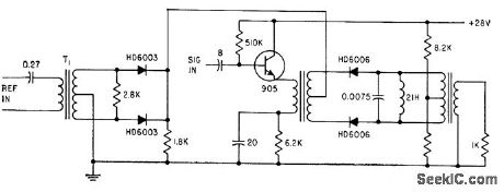
DIFFERENTIAL_TRANSFO_RMER_TRANSDUCER
Published:2009/7/23 23:19:00 Author:Jessie
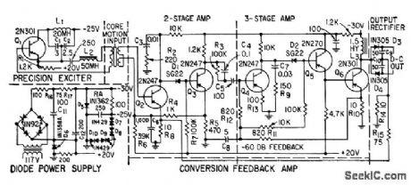
Detects and responds with 0.1% linearity to core displacement. Low-level ac transformer output is converted to 10 to 50 ma d-c transmission signal with : w maximum power by high-input-impedance feedback amplifier. Precision exciter consists of constant-voltage 1-kc oscillator and high-Q swamping choke. Gain is stabilized by using separate d-c feedback loop for each group of d-c coupled transistors.-L. H. Dulberger, Constant-Current Technique Cuts Servo Response Time, Electronics, 32:28, p 52-54. (View)
View full Circuit Diagram | Comments | Reading(541)
PENTODE_COMMON_PLATE_MIXER
Published:2009/7/23 23:18:00 Author:Jessie
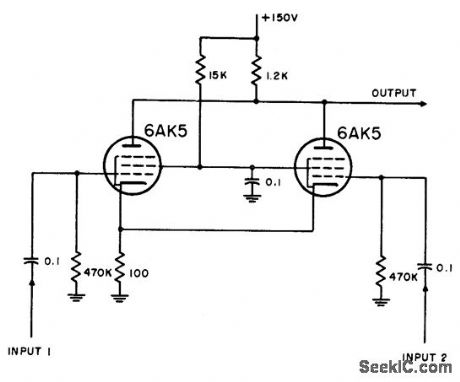
Circuit is good adder for coincident inputs. Operates best with positive input pulses and negative going output.-NBS, Handbook Preferred Circuits Navy Aeronautical Electronic Equipment, Vol. 1, Electron Tube Circuits, 1963, p N4-7. (View)
View full Circuit Diagram | Comments | Reading(660)
Very_wide_range_V_F_converter
Published:2009/7/23 23:18:00 Author:Jessie

Fig. 12-4 This circuit is a highly modified version of the circuit in Fig. 12-3 and it features a range from 1 Hz to 30 MHz. The circuit maintains a 0.08% linearity over the entire range with a full-scale drift of about 20 ppm/℃. Zero-point error is 0.3 Hz/℃ (and is directly related to the 50 nV/℃ drift specification of the LTC1052). To trim, ground the input and adjust the 1-Hz trim until oscillation just starts. Next, apply 3.000 V and set the 30-MHz trim for a 30.00-MHz output. Repeat the procedure until both points are fixed. Linear Technology Linear Applications Handbook 1990, p AN9-15. (View)
View full Circuit Diagram | Comments | Reading(539)
MARKER_IFF_MIXER
Published:2009/7/23 23:18:00 Author:Jessie
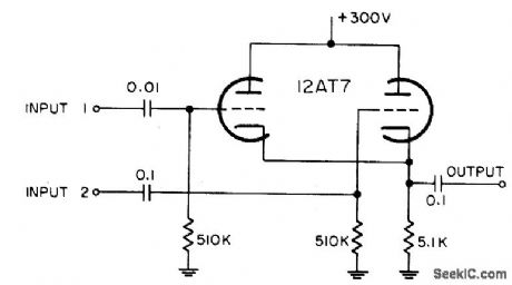
Combines 9-v positive markers with ill signals from 2 to 10 v.-NBS, Handbook Preferred Circuits Navy Aeronautical Electronic Equipment, Vol.1, Electron Tube Circuits, 1963, p N4-2. (View)
View full Circuit Diagram | Comments | Reading(766)
Improved_linear_current_regulator
Published:2009/7/23 23:18:00 Author:Jessie

This circuit is similar to that of Fig. 7-13, except that the addition of C1 prevents oscillation. (View)
View full Circuit Diagram | Comments | Reading(539)
RANGE_STROBE_MARKER_MIXER
Published:2009/7/23 23:17:00 Author:Jessie
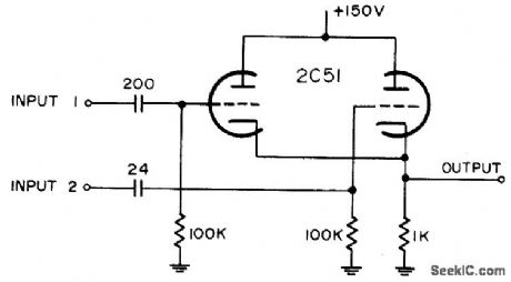
Common-cathode dual-triode video mixer is used for combining two positive-polarity radar range strobe markers.-NBS, Handbook Preferred Circuits Navy Aeronautical Electronic Equipment, Vol. 1, Electron Tube Circuits, 1963, p N4-2. (View)
View full Circuit Diagram | Comments | Reading(508)
Chopper_stabilized_instrumentation_arnplifier
Published:2009/7/23 23:17:00 Author:Jessie
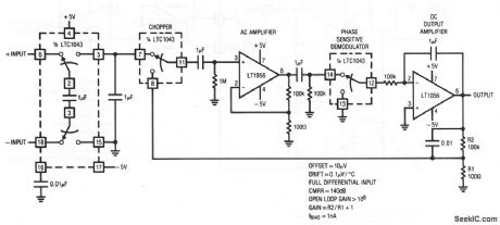
This circuit is similar to that of Fig. 1-4, but uses the remaining LTC1043 (Fig. 1-4B) section to form a low-drift chopper amplifier. The approach maintains the true differential inputs, while achieving 0.1-μV/℃ drift. (View)
View full Circuit Diagram | Comments | Reading(787)
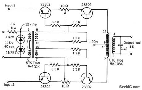
4_W_CLASS_B_SERVO_AMPLIFIER
Published:2009/7/23 23:17:00 Author:Jessie

Gives power gain of 42 db. Voltage amplification is constant within 2.5 db of 42.5 db. Transformer data is for 400-cps operation. -Texas Instruments Inc., Transistor Circuit Design, McGraw-Hill, N.Y., 1963, p 241. (View)
View full Circuit Diagram | Comments | Reading(719)
Simple_5_V_adjustable_regulator
Published:2009/7/23 23:17:00 Author:Jessie

This circuit is similar to that of Fig. 7-24, except that the output is adjustable (above 5 V). (View)
View full Circuit Diagram | Comments | Reading(505)
DIFFUSED_BASE_GERMANIUM_VIDEO_AMPLIFIER
Published:2009/7/23 23:17:00 Author:Jessie
Use of standard stability criteria for wideband amplifiers gives current gain of 34 db up to 50 Mc when using any diffused base germanium mesa transistor similar to 2N2415. D-c biasing uses both series and shunt feedback to each stage, enabling circuit bandwidth to be extended to d-c if necessary.-Texas Instruments Inc., Transistor Circuit Design, McGraw-Hill, N.Y., 1963, p 268. (View)
View full Circuit Diagram | Comments | Reading(664)
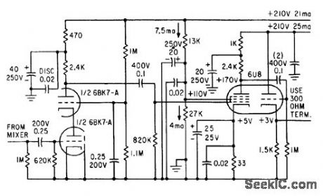
PREFERRED_INTERMEDIATE_LEVEL_AMPLIFIER_1
Published:2009/7/23 23:22:00 Author:Jessie
Designed to amplify 1-v signal, such as output of mixer or cathode follower, to level required for input to video driver. Amplification of 3 to 5 may be increased by cascading. Use of R5 and C4 is optional.-NBS, Handbook Preferred Circuits Navy Aeronautical Electronic Equipment, Vol. I, Electron Tube Circuits, 1963, PC 26, p 26-2. (View)
View full Circuit Diagram | Comments | Reading(654)
IC_amplifier_with_high_current_booster
Published:2009/7/23 23:22:00 Author:Jessie
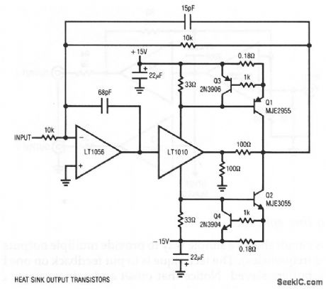
This circuit is capable of delivering a 3-A output current (±10 V) with a bandwidth of 100kHz, and a slew-rate of about 10 V/μs. (View)
View full Circuit Diagram | Comments | Reading(912)
3_A_positive_fixed_voltage_regulator
Published:2009/7/23 23:21:00 Author:Jessie

The LAS1400 series voltage regulators are ICs that contain all elements necessary for linear regulation (safe-area protection, thermal overload, current limiting, as shown in Fig. 7-28C). Figure 7-28B shows the output voltage and tolerance for the various LAS1400 part numbers. Figure 7-28D shows the absolute maximum ratings. (View)
View full Circuit Diagram | Comments | Reading(576)
QUADRATURE_VOLTAGE_REJECTION
Published:2009/7/23 23:21:00 Author:Jessie
Suppresses quadrature voltages in servo loops while delivering in-phase a-c signal. Phase reference voltage controls two unmatched diodes so they conduct only when in-phase signal component is passing through maximum and quadrature is passing through minimum. Prevents overload of amplifier.-B. Fennick, Phase-Selective Gate Rejects Quadrature, Electronics, 31:51, p 89-91. (View)
View full Circuit Diagram | Comments | Reading(491)
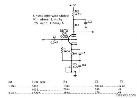
HIGH_GAIN_VIDEO_PREAMP
Published:2009/7/23 23:21:00 Author:Jessie
Used in microwave interferometer system when additional gain is required along with 3.Mc bandwidth.-H. L. Bunn, Determining Electron Density and Distribution in Plasmas, Electronics, 34:14, p 71-75. (View)
View full Circuit Diagram | Comments | Reading(586)
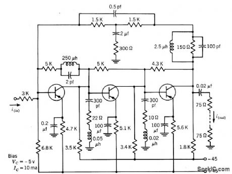
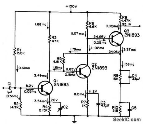
DIGITAL_SERVO_MODULATOR
Published:2009/7/23 23:20:00 Author:Jessie
Used to subtract two analog currents of digital-to-analog converter, giving phase-sensitive 60-cps square-wave output signal. Modulator is driven from 60-cps line to maintain precise phase relationship with two-phase servo motor. Modulator gives 2.4.mV p-p output signal for 2-microamp input signal on one side, and 1.1 V pp for 1-ma input signal on one side. First output corresponds to least significant digit error in Gray-to-binary converter, and latter to most significant digit error.-Texas Instruments Inc., Transistor Circuit Design, McGraw-Hill, N.Y., 1963, p 492. (View)
View full Circuit Diagram | Comments | Reading(577)
Fast_V_F_converter
Published:2009/7/23 23:20:00 Author:Jessie

Fig. 12-5 This circuit features a range from 1 Hz to 10 MHz with a linearity of 0.06%, and a typical full-scale drift of 50 ppm/℃. The zero-point error is about 0.2 μV/℃ (or 0.2 Hz/℃). To trim, ground the input and adjust the 1-Hz trim for 1-Hz output. Next, apply 10.000 V and adjust the gain trim for 10.000-MHz output. Repeat the procedure until both points are fixed. Linear Technology, Linear Applications Handbook, 1990 p AN13-9. (View)
View full Circuit Diagram | Comments | Reading(584)
Simple_video_line_splitter_
Published:2009/7/23 23:20:00 Author:Jessie

This circuit shows a simple way to provide multiple outputs for a single input (at video frequencies). The technique is to put feedback on one buffer, with the remaining buffers slaved. Notice that offset and gain accuracy of the slave buffers depends on the matching with the master. (View)
View full Circuit Diagram | Comments | Reading(2645)
PREFERRED_HIGHLEVEL_AMPLIFIER
Published:2009/7/23 23:20:00 Author:Jessie
Linear pulse voltage amplifier, designed primarily as crt intensity modulation device, has minimum bandwidth of 3 Mc. Takes positive input pulses and gives maximum negative output of 55 v.-NBS, Handbook Preferred Circuits Navy Aeronautical Electronic Equipment, Vol. II, Semiconductor Device Circuits, PSC 20 (originally PC 220), p 20-2. (View)
View full Circuit Diagram | Comments | Reading(586)
| Pages:1111/2234 At 2011011102110311041105110611071108110911101111111211131114111511161117111811191120Under 20 |
Circuit Categories
power supply circuit
Amplifier Circuit
Basic Circuit
LED and Light Circuit
Sensor Circuit
Signal Processing
Electrical Equipment Circuit
Control Circuit
Remote Control Circuit
A/D-D/A Converter Circuit
Audio Circuit
Measuring and Test Circuit
Communication Circuit
Computer-Related Circuit
555 Circuit
Automotive Circuit
Repairing Circuit