
Measuring and Test Circuit
Index 80
LOGIC_CHIP_TESTER
Published:2009/6/18 23:46:00 Author:May

This device compares two logic signals and indicates whether the two logic signals are the same or different. To use the tester, first connect the test input to the suspect pin of the DUT. Next, con-nect the reference input to the same pin of an identical reference chip that is known to be good. Push the reset button to begin the test; the green section of the bicolor LED will be illuminated. Any sig-nal on the test device that differs from the one on the reference device will then mornentarily light the LED lamp that corresponds to that pin, and also latch on the red section of the bi-color LED. That indicates that the device under test is faulty. If the reference and DUT signals are the same, the DUT is OK, and the green LED will remain lit. (View)
View full Circuit Diagram | Comments | Reading(1056)
1_kW_POWER_METER
Published:2009/6/18 23:40:00 Author:May
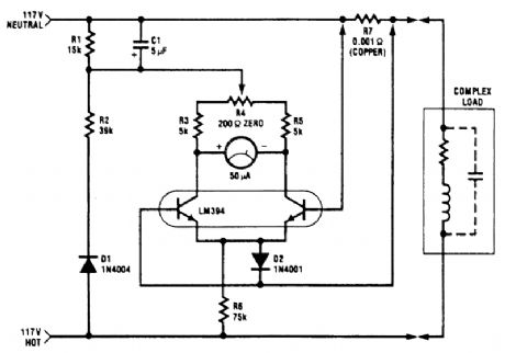
The power meter shown uses only one transistor pair to provide the complete (X)(Y)function.The circuit is intended for 117 Vac±50 Vac operation, but can be easily modified for higher or lower voltages. It measures true (nonreactive)power being delivered to the load and requires no external power supply. Idling power drain is only 0.5W. The load current-sensing voltage is only 10 mV, keep-ing load voltage loss to 0.01%. Rejection of reactive load currents is better than 100:1 for linear loads.Nonlinearity is about 1% full scale when using a 50-μA meter movement. The temperature correction for gain is accomplished by using a copper shunt (+0.32%/℃) for load-current sensing. This circuit measures power on negative cycles only, so it cannot be used on rectifying loads. (View)
View full Circuit Diagram | Comments | Reading(1489)
NEGATIVE_REFERENCE_VOLTAGE_CIRCUIT
Published:2009/6/18 23:19:00 Author:May

This figure illustrates a circuit that supplies a precise negative reference voltage. To meet requirements of accuracy and stability, it incorporates a highly precise positive reference voltage by use of a high-gain, stable feedback booster circuit.The booster circuit includes an operational amplifier and a transistor, which handles the load current. Typically, a po sitive-reference-voltage circuit can handle only relatively small load currents.This consideration does not apply in the present circuit because the p ositive-refer ence-voltage unit is placed in the voltage feedback loop of the booster circuit in parallel with resistor RB. Thus, from the perspective of the p o sitive-reference-v oltage unit,RB is a constant load. This feature enhances the stability of the circuit by removing the load regulation factor.Provided that the offset voltage of the operational amplifier is low, the accuracy of the overall circuit depends only on the accuracy of the p ositive-refer ence-voltag e unit. The overall circuit draws very little power for its own operation. It can handle unexpectedly heavy loads; the feedback conftg-uration and the high gain provided by the combination of the operational amplifier and the transistor give the circuit a very low output impedance. The capacitors reduce the noise voltage and help stabilize the circuit. In the event that the load becomes a short circuit, RD, protects the transistor by lim-iting the load current. (View)
View full Circuit Diagram | Comments | Reading(695)
INDUCTANCE_WITH_DVM_MEASURING_CIRCUIT
Published:2009/6/18 23:10:00 Author:May

The inductance meter comprises an oscillator and pulse shaper. The square wave from the oscillator is differentiated and the differentiator output is shaped and read on a DVM. This will be proportional to inductance. R1A, B, C set calibration and R6 is an offset control. (View)
View full Circuit Diagram | Comments | Reading(1727)
SINGLE_CHIP_DIGITAL_VOLTMETER
Published:2009/6/18 23:04:00 Author:May
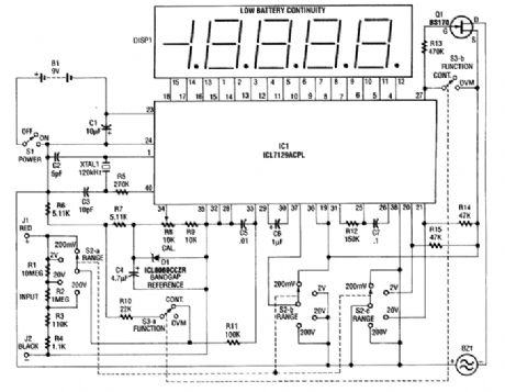
This 4 1/2-digit DVM circuit is built around a Maxim ICL7129ACPL A/D converter and LCD driver. An ICL8069 CCZR 1.2-V band-gap reference diode is used for a voltage reference. S2a-b-c select one of four ranges up to 200 V (maximum). The meter also has a piezoelectric buzzer for continuity testing. S3 selects either DVM or continuity. Crystal 1 can be changed to 100 kHz if maximum rejection of 50 Hz is desired. The crystal normally provides 120 kHz for best 60-Hz rejection. This is caused by the dual-slope conversion technique used in IC1. (View)
View full Circuit Diagram | Comments | Reading(1392)
POPULAR_ELECTRONICS
Published:2009/6/18 22:53:00 Author:May

The electronic level uses a pa:r ofphototransistors and an infrared LED to sense bubble position In this circuit,the amounts of infrared radiation received by phototransistors Q1 and Q2 are translated by op-amp U1 and dual-timer U2 into either a steady tone,or a fast-or slow-pulsing one. (View)
View full Circuit Diagram | Comments | Reading(0)
VCR_HEAD_AMPLIFIER_TESTER
Published:2009/6/18 21:52:00 Author:May
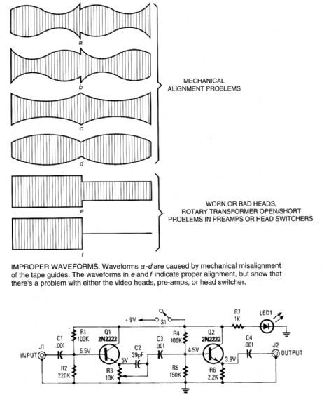
This amplifier enables you to use a signal from a working VCR to test the head amplifiers of a suspected defective VCR.The circuit is basically a video amtplifier. (View)
View full Circuit Diagram | Comments | Reading(593)
SAMPLE_AND_HOLD_CIRCUIT_II
Published:2009/6/18 21:25:00 Author:May
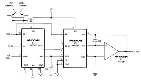
Driving a D/A converter with an A/D converter provides an overall analog-hold function, which though limited in output resolution, offers zero voltage droop and infinite hold time. The A/D converter shown (ICl) includes a 12-bit compatible track/hold at its input. The track/hold specifies a 6-MHz full-power bandwidth, a 30-ns aperture delay, and a 50-ps aperture jitter. The direct connections shown al-low the D/A converter to reconstruct signal levels within the input range of 0 to 5 V. (View)
View full Circuit Diagram | Comments | Reading(0)
SAMPLE_AND_HOLD_CIRCUIT_I
Published:2009/6/18 21:23:00 Author:May

This circuit demonstrates the principle of the sample-and-hold circuit. S1 can be replaced by electronic switches (FET, etc.) in an actual application. (View)
View full Circuit Diagram | Comments | Reading(529)
TESTS_DRIVER_FOR_HOBBY_SERVOS
Published:2009/6/18 4:32:00 Author:May
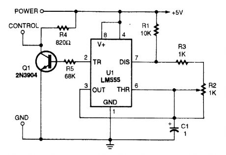
This circuit will generate the pulse used to control hobby servos. With the components shown the servo should produce a 90° total rotation. (View)
View full Circuit Diagram | Comments | Reading(775)
DUMMY_LOAD_AND_VIDEO_DETECTOR_FOR_TRANSMITTER_TESTS
Published:2009/6/18 4:29:00 Author:May
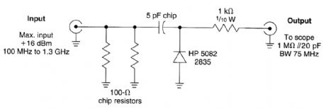
This circuit is useful as a video modulation monitor for testing low-power video transmitters. For higher power inputs, use a suitable attenuator between the detector and the source. The detector should be connected to scope with as short a cable as possible to preserve video bandwidth. (View)
View full Circuit Diagram | Comments | Reading(626)
VOICE_LEVEL_METER
Published:2009/6/18 4:24:00 Author:May

Using an LM3915 VU meter LED bar graph driver,10 LEDs are driven。A simple audio amplifierdrives a detector circuit,which provides dc drive for the LM3915. (View)
View full Circuit Diagram | Comments | Reading(6077)
BAR_GRAPH_LEVEL_GAUGE
Published:2009/6/18 4:20:00 Author:May
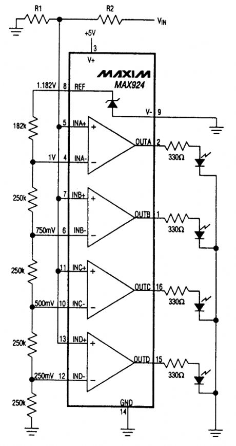
A quad comparator and divider network form a 4-level comparator that drives 4 LEDs. RI and R2 can be used to scale the basic sensitivity of 250 mV/LED to higher voltages than the basic 1 volt (for all 4 LEDs lit). (View)
View full Circuit Diagram | Comments | Reading(0)
HIGH_EFFICIENCY_DISPLAY_CONTRAST_AND_BACKLIGHT_CONTROL
Published:2009/6/18 4:19:00 Author:May

The LT1182 and LT1183 are compact high-performance solutions for powering LCD screens used in portable computers and instruments. Backlight control using a Cold Cathode Fluorescent lamp (CCFL) is accomplished with a switching regulator at efficiencies up to 90%. A second switch-ing regulator converts the positive input to either positive or negative bias voltages used for LCD contrast control. Both regulators allow full range of adjustment using a D/A converter, PWM or po-tentiometer control. Grounded bulb configurations are also easily controlled with minimal parts count. The 200-kHz switching frequency minimizes the size of transformers and external compo-nents. A shutdown mode powers down both regulators and reduces supply current to just 35 μA. (View)
View full Circuit Diagram | Comments | Reading(1152)
ac_NOISE_DETECTOR
Published:2009/6/18 4:04:00 Author:May

This circuit can be added to the glitch detector to trigger on ac noise. (View)
View full Circuit Diagram | Comments | Reading(759)
455_kHz_AM_DETECTOR
Published:2009/6/18 4:03:00 Author:May

The LTC1278 undersamples the 455-kHz carrier to recover the 5-kHz modulating signal. The ap-plication shown uses the LTC1278 to undersample (at 227.5 ksps) a 455-kHz IF amplitude-modu-lated by a 5-kHz sine wave. Figures 26-19A and 26-19B show, respectively, the 455-kHz IF carrier and the recovered 5-kHz sine wave that results from a 12-bit DAC reconstruction. (View)
View full Circuit Diagram | Comments | Reading(757)
POSITIVE_PEAK_DETECTOR
Published:2009/6/18 4:01:00 Author:May

View full Circuit Diagram | Comments | Reading(0)
NEGATIVE_PEAK_DETECTOR
Published:2009/6/18 4:01:00 Author:May

View full Circuit Diagram | Comments | Reading(0)
LOW_DRIFT_PEAK_DETECTOR
Published:2009/6/18 4:00:00 Author:May

View full Circuit Diagram | Comments | Reading(0)
AIR_FLOW_DETECTOR
Published:2009/6/18 3:59:00 Author:May

View full Circuit Diagram | Comments | Reading(0)
| Pages:80/101 At 206162636465666768697071727374757677787980Under 20 |
Circuit Categories
power supply circuit
Amplifier Circuit
Basic Circuit
LED and Light Circuit
Sensor Circuit
Signal Processing
Electrical Equipment Circuit
Control Circuit
Remote Control Circuit
A/D-D/A Converter Circuit
Audio Circuit
Measuring and Test Circuit
Communication Circuit
Computer-Related Circuit
555 Circuit
Automotive Circuit
Repairing Circuit