Measuring and Test Circuit
NEGATIVE_REFERENCE_VOLTAGE_CIRCUIT
Published:2009/6/18 23:19:00 Author:May | From:SeekIC
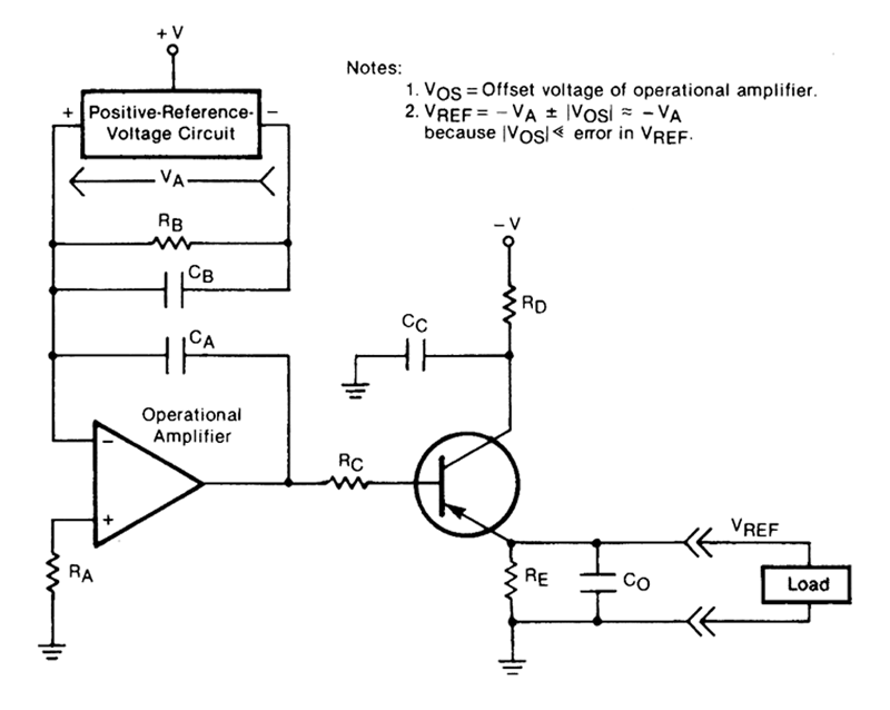
This figure illustrates a circuit that supplies a precise negative reference voltage. To meet requirements of accuracy and stability, it incorporates a highly precise positive reference voltage by use of a high-gain, stable feedback booster circuit.The booster circuit includes an operational amplifier and a transistor, which handles the load current. Typically, a po sitive-reference-voltage circuit can handle only relatively small load currents.This consideration does not apply in the present circuit because the p ositive-refer ence-voltage unit is placed in the voltage feedback loop of the booster circuit in parallel with resistor RB. Thus, from the perspective of the p o sitive-reference-v oltage unit,RB is a constant load. This feature enhances the stability of the circuit by removing the load regulation factor.Provided that the offset voltage of the operational amplifier is low, the accuracy of the overall circuit depends only on the accuracy of the p ositive-refer ence-voltag e unit. The overall circuit draws very little power for its own operation. It can handle unexpectedly heavy loads; the feedback conftg-uration and the high gain provided by the combination of the operational amplifier and the transistor give the circuit a very low output impedance. The capacitors reduce the noise voltage and help stabilize the circuit. In the event that the load becomes a short circuit, RD, protects the transistor by lim-iting the load current.
Reprinted Url Of This Article:
http://www.seekic.com/circuit_diagram/Measuring_and_Test_Circuit/NEGATIVE_REFERENCE_VOLTAGE_CIRCUIT.html
Print this Page | Comments | Reading(3)

Article Categories
power supply circuit
Amplifier Circuit
Basic Circuit
LED and Light Circuit
Sensor Circuit
Signal Processing
Electrical Equipment Circuit
Control Circuit
Remote Control Circuit
A/D-D/A Converter Circuit
Audio Circuit
Measuring and Test Circuit
Communication Circuit
Computer-Related Circuit
555 Circuit
Automotive Circuit
Repairing Circuit
Code: