
Circuit Diagram
Index 1786
The switch circuit with functions of self-lock (auto keeping) (2)
Published:2011/6/10 21:02:00 Author:qqtang | Keyword: switch circuit, self-lock
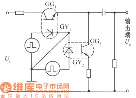
In the figure is the application in modulation (or wave chopper)of photoelectric couplers. Impose two square wave voltages, between which the difference is 180o, on GY1 and GY2 of the photoelectric coupler, so that they glow in turn, the light dependent triodes of GG1 and GG2 are conducting and blocked in turn, the output terminal gets periodical signals, which fulfills functions of modulation on the input signal Ui. (View)
View full Circuit Diagram | Comments | Reading(989)
The construction circuit of heat-release electric infrared sensor
Published:2011/6/10 21:30:00 Author:qqtang | Keyword: construction circuit, infrared sensor

Figure: The construction circuit of heat-release electric infrared sensor (View)
View full Circuit Diagram | Comments | Reading(448)
The simplest multi-oscillator circuit of photoelectric couplers
Published:2011/6/10 20:52:00 Author:qqtang | Keyword: multi-oscillator circuit, photoelectric couplers
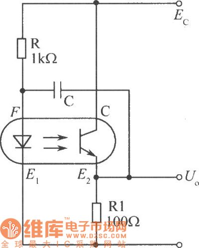
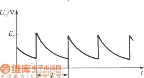
In the figure is simplest multi-oscillator circuit of photoelectric couplers. When the power is on, as the voltages on the two terminals of capacitor C can mutate and the resistance of resistor R is higher than RL, so the power supply voltage is mainly imposed on R, and the LEV on F is low, the LED is blocked, as the charging voltage of the capacitor increases, the LEV of F is rising. when the LEV rises to a certain value, the LED is conducting and glowing, the light dependent pipe is conducting, the output voltage is jumping and close to the voltage of the power supply.
(View)
View full Circuit Diagram | Comments | Reading(1001)
The single steady circuit of photoelectric couplers
Published:2011/6/10 21:03:00 Author:qqtang | Keyword: single steady circuit, photoelectric couplers

View full Circuit Diagram | Comments | Reading(793)
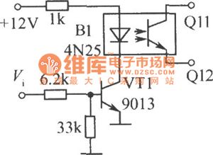
The high voltage steady circuit of photoelectric couplers
Published:2011/6/10 8:42:00 Author:qqtang | Keyword: high voltage, steady circuit, photoelectric couplers

As is indicated in the figure, common drive pipes are high voltage transistors( in the figure, the drive pipe is 9013). When the output voltage increases, the bias voltage of VT55 is stepping up, which makes the positive current of the LED in B5 increase and the voltages between light dependent pipes reduce, and the bias voltage on the adjusting pipe reduces but the internal resistance increases, so the output voltage reduces; on the contrary, the output voltage steps up, so that the output voltage is kept steady. (View)
View full Circuit Diagram | Comments | Reading(818)
The auto light control circuit of photoelectric couplers
Published:2011/6/10 8:31:00 Author:qqtang | Keyword: control circuit, photoelectric couplers
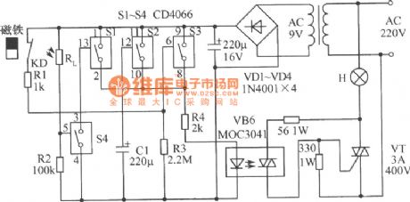
See as the circuit, in the 4 teams of analog electric switches(SI~S4), S1, S2 and S3 are in parallel connection, and they are used in the time delaying circuit, when they are connected with the power supply, they drive the dual-way transistor VT by R4 and VB6, VT directly control the hall lights; S4 and the external light dependent resistor RL form the outside ray detection circuit. When the door is closed, the closed type dry reed pipe KD, which is installed on the door frame, is affected by the magnet and it cut off, then S1, S2 and S3 are in open state. When the owner comes home at night, the magnet is away from KD, the KD touch spot is closed. (View)
View full Circuit Diagram | Comments | Reading(1298)
The connector circuit of photoelectric couplers
Published:2011/6/10 8:18:00 Author:qqtang | Keyword: connector circuit, photoelectric couplers
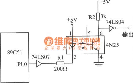
See as the circuit, the photoelectric coupler 4N25 performs the functions of coupling pulse signals and separating single chip computer 89C51 system from its output part, which makes the two parts separated. The output part of the ground wire connects with the shell and the earth, the power supply ground wire of 89C51 system is suspended, which is not connected with ground wire of the AC power supply, so that the power supply change of the output part has little effect on the single chip computer power supply, the effect on the small system is reduced, and the reliability of the system is increased. (View)
View full Circuit Diagram | Comments | Reading(1048)
The switch circuit of photoelectric couplers (2)
Published:2011/6/10 7:58:00 Author:qqtang | Keyword: switch circuit, photoelectric couplers
View full Circuit Diagram | Comments | Reading(788)
DC high background circuit elimination circuit
Published:2011/5/30 4:52:00 Author:chopper | Keyword: DC, high background circuit, elimination
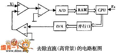
Because the output signal of infrared CCD is of high background and wide dynamic range,it is essential to eliminate the DC high background and automatic gain for smoothing the background noise as well as extracting target signal in this signal's processing circuit.It introduces some normal methods for the application on this signal procession by analyzing the design requirements of infrared CCD signal.At last,it stresses the integration design method on CCD signal processing circuit based on CPLD and VSP3010.
(View)
View full Circuit Diagram | Comments | Reading(369)
The AND gate logic circuit of photoelectric couplers
Published:2011/6/10 7:49:00 Author:qqtang | Keyword: AND gate, photoelectric couplers

View full Circuit Diagram | Comments | Reading(879)
simple and practical three-key interlock electronic switch circuit
Published:2011/5/29 6:58:00 Author:chopper | Keyword: simple and practical, three-key interlock, electronic switch

View full Circuit Diagram | Comments | Reading(743)
The switch circuit of photoelectric couplers (1)
Published:2011/6/10 7:57:00 Author:qqtang | Keyword: switch circuit, photoelectric couplers
View full Circuit Diagram | Comments | Reading(819)
single-supply,low-voltage,low-consumption operational amplifier circuit
Published:2011/5/29 7:20:00 Author:chopper | Keyword: single-supply, low-voltage, low-consumption, operational amplifier

This is a single-supply,low-voltage,low-consumption operational amplifier circuit.The operational amplifier can choose low-voltage series,such as OPA2350,MAX412,OPA2344 and so on.If the supply voltage is 5V,the resistance with * would be 42K;and if the supply voltage is 3.3V,please choose a resistance with 27K.
(View)
View full Circuit Diagram | Comments | Reading(1862)
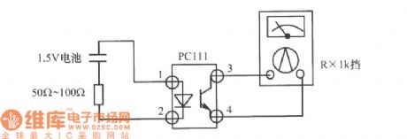
The digital multimeter test circuit of photoelectric coupler
Published:2011/6/10 7:55:00 Author:qqtang | Keyword: digital multimeter, photoelectric coupler
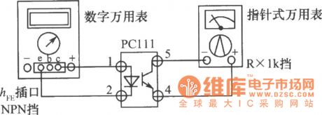
View full Circuit Diagram | Comments | Reading(760)
TA7641 wired interphone circuit
Published:2011/5/28 1:29:00 Author:chopper | Keyword: wired interphone

We can make a wired interphone easily by using a single chip IC TA7641 in AM radio.The interphone circuit is shown as follows.The interphone is formed by A and B.A is the host,and B is extension.Actually,B is a speaker B2.A and B is connected by twinax cable.When plug XP is inserted to socket XS,the interphone runs.Switch S is a talkback transfer switch.As the following picture,A is in speech state, and B is for obedient state.
(View)
View full Circuit Diagram | Comments | Reading(1388)
The effect judgement circuit of photoelectric couplers
Published:2011/6/10 7:52:00 Author:qqtang | Keyword: effect judgement, photoelectric couplers
View full Circuit Diagram | Comments | Reading(828)
DS14185 data interface driver/receiver combination circuit
Published:2011/5/25 21:15:00 Author:Christina | Keyword: data interface, driver, receiver, combination

The DS14185 is composed of three drivers and five receivers, it has the DC-DC converter and does not need the +12V power supply. The DS14185 has the noise filter inside, so there is no need to add the rate conversion filter capacitance. The DS14185 can be used in the applications of the data terminal equipment (DTE) and the data circuit terminal equipment (DCE). The drive input port and the receiver output port is compatible with the TTL or CMOS circuit. From the data terminal equipment (DTE)'s transmission interface to the data circuit terminal equipment (DCE)'s transmission interface, there are nine pins, among them there are two data lines and six control lines. The data lines are the TXD and RXD, and the control line are the RTS、DTR、DSRT、DCE、CTS、RI. The DS14185 supplies the DTE interface, the wiring method is as shown in the figure. (View)
View full Circuit Diagram | Comments | Reading(584)
The 9-bit LED LEV displaying drive circuit of LB1409
Published:2011/6/10 5:00:00 Author:qqtang | Keyword: 9-bit LED, drive circuit

In the figure is the 9-bit LED LEV displaying drive circuit of LB1409. Figure (a) is the LEV display drive circuit which consists of LV1409, figure (b) is the LEV display drive circuit of application reference voltage. LB1409 is produced by Toyo, Japan, and the local products, such as D1409 and SL1409, are like it, and they can replace it. The LB1409 input pole is indicated with 9 stick-shape red or green LED. Inside the circuit, there is a DC amplifier, whose gains can be changed by external resistors. (View)
View full Circuit Diagram | Comments | Reading(1311)
450Hz Venturi bridge signal generator circuit
Published:2011/5/25 6:06:00 Author:Christina | Keyword: 450Hz, Venturi, bridge signal, generator
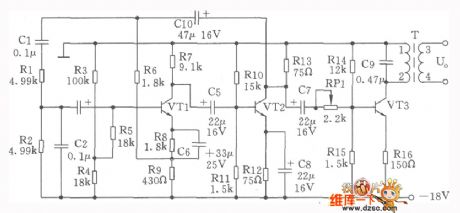
The 450Hz Venturi bridge signal generator circuit, also called the RC oscillator, the circuit is as shown. The oscillator is composed of the VTl, VT2, the feedback network Rl, R2 and the C1、C2. The negative feedback which is composed of the R6、R9 and Cl0 keeps the stabilization of the amplitude and the frequency. The transistor VTl's DC bias resistor are the R3, R4, R7, R8 and R9. The R5 is the input addition resistor, it improves the input impedance. The Rl0, Rll, Rl2 and Rl3 are the DC bias resistor of VT2. VT3 is the power output stage, the output signal gets through the frequency selection networks C9 and L1-2, then output by the transformer T's secondary stage L3-4. The transistor VTl~VT3:3DG128、β=50~70. The capacitor Cl, C2: CM0-100V-50000pF, the measurement error ±0.3%. The thermistor RT: RR527B uses the 2.2V, 12mA.
(View)
View full Circuit Diagram | Comments | Reading(842)
The LEV display drive circuit of the TA7666P dual-line 5-bit LED
Published:2011/6/12 0:06:00 Author:qqtang | Keyword: LEV display, drive circuit
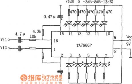
In the figure is the LEV display drive circuit of the TA7666P dual-line 5-bit LED. The integrated circuit of TA7666P is produced by Toshiba, the local products of TB7666P, XG7666P and so on are like it and can substitute it directly. (View)
View full Circuit Diagram | Comments | Reading(2697)
| Pages:1786/2234 At 2017811782178317841785178617871788178917901791179217931794179517961797179817991800Under 20 |
Circuit Categories
power supply circuit
Amplifier Circuit
Basic Circuit
LED and Light Circuit
Sensor Circuit
Signal Processing
Electrical Equipment Circuit
Control Circuit
Remote Control Circuit
A/D-D/A Converter Circuit
Audio Circuit
Measuring and Test Circuit
Communication Circuit
Computer-Related Circuit
555 Circuit
Automotive Circuit
Repairing Circuit