
Index 324
Ratiometic_conversion
Published:2009/7/25 4:32:00 Author:Jessie

Figure 9-4 shows the ADC0816/17 connected for ratiometric conversion. Becauseboth ends of the 256R resistor ladder are available externally (Fig.9-1) the ICs areideally suited for use with ratiometric transducers A ratiometric transducer is aconverslon device in which the output is proportional to so me arbitrary full-scalevalue.The actual value of the transducer output is of no great importance but theratio of this output to the full-scale reference is valuable.The prime advantage of a ratiometric transducer is that an accurate reference is not essential However the reference should be nolse free because the voltage spikes during a converslon could cause inaccurate results.The circuit of Fig.9-4 uses the existing 5-V supply for reference thus eliminating the need for a special external reference. Take careto reduce power-supply nolse,The supply lines should be bypassed and separate PC traces shodld be used to route the 5-V and ground to the reference inputs andto the supply pms (if practical). NATIONAL SEMICONDUCTOR APPLICATION NOTE258 1994. P.592.
(View)
View full Circuit Diagram | Comments | Reading(565)
FIELD_STRENGTH_AT_7_MHz
Published:2009/6/28 22:04:00 Author:May

Operates from single dry cell, Meter can be calibrated in decibels with Hewlett-Packard 606A or equivalent signal generator,Jack permits remote metering L1 is 5 turns、and L2 is 30 turns wound onAmidonT68-2 core.-R,W Jones、A7-MHz Vertical Parasitic Array QST,Nov,1973、p 39-43and 52 (View)
View full Circuit Diagram | Comments | Reading(651)
SELECTABLE_BANDWIDTH_NOTCH_FILTER
Published:2009/6/28 22:02:00 Author:May


Circuit Notes
This notch filter, which operates at up to 200 kHz, uses a modified Wien bridge to select bandwidth over which frequencies are rejected. RC components determine filter's center frequency, Plselects notch bandwidth. Notch depth is fixed at about 60 dB. (View)
View full Circuit Diagram | Comments | Reading(939)
VARIABLE_ZENER_DIODE
Published:2009/6/28 22:01:00 Author:May

The circuit behaves like a zener diode over a large range of voltages. The current passing through the voltage divider R1-R2 is substantially larger than the transistor base current and is in the region of 8 mA. The stabilizing voltage is adjustable over the range 5-45 V by changing the value of R2. The total current drawn by the circuit is variable over the range 15 mA to 50 mA. This value is determined by the maximum dissipation of the zener diode. In the case of a 250 mW device, this is of the order of 50 mA. (View)
View full Circuit Diagram | Comments | Reading(201)
INSTANT_VSWR_BRIDGE
Published:2009/6/28 22:01:00 Author:May


Modified 190B Tektronix constant-amplitude signal generator is combined with 50-ohm resistance bridge toglve stable high-accuracy instrument for measuring voltage standing-wave ratio as guide fortuning antennas Range iS 160 meters through 10 meters,Trim Rx so incident or forward voltage at position 1 of S1 equals reflected voltage at position 2. Article gives chart for finding VSWR. Step-by-step procedure for modifying signal generator is given.-D.Sander, Make Antenna Tuning a Joy, 73 Magazine, May 1978, p 134-136. (View)
View full Circuit Diagram | Comments | Reading(977)
74 Series digital circuit of 74195,74LS195A 4-bit parallel access shift register
Published:2011/8/1 0:56:00 Author:Lucas | Keyword: 74 Series, digital circuit , 4-bit parallel access , shift register

The typical maximum clock frequency of 74195,74 LS195A is 39MHz, and 74S195 is 105MHz; the typical operating frequency of 74HC195 is 45Hz.
a, b, c, d = the corresponding steady input level of A, B, C, D. QA0, QB0, QC0, QD0= the corresponding level of QA, QB, QC, QD before the establishment of steady-state input conditions. QAn, QBn, QCn= the corresponding level of QA, QB, QC at the latest time hopping.
(View)
View full Circuit Diagram | Comments | Reading(3494)
THREE_AMPLIFIER_NOTCH_FILTER(OR_ELLIPTIC_FILTER_BUILDING_BLOCK)
Published:2009/6/28 21:58:00 Author:May


View full Circuit Diagram | Comments | Reading(608)
74 Series digital circuit of 74194,74LS194A 4-bit two-way general shift register
Published:2011/8/1 0:53:00 Author:Lucas | Keyword: 74 Series , digital circuit , 4-bit two-way , general shift register


The typical maximum clock frequency of 74197,74 LS194A is 36MHz, and 74S194 is 104MHz; the typical operating frequency of 74HC194 is 45Hz.
a, b, c, d = the corresponding steady input level of A, B, C, D. QA0, QB0, QC0, QD0= the corresponding level of QA, QB, QC, QD before the establishment of steady-state input conditions. QAn, QBn, QCn= the corresponding level of QA, QB, QC at the latest time hopping.
(View)
View full Circuit Diagram | Comments | Reading(3126)
FREQUENCY_DIVIDER_CHAIN
Published:2009/6/28 21:54:00 Author:May

Circuit NotesSawtooth output from each stage IS one half frequency of preceding stage. (View)
View full Circuit Diagram | Comments | Reading(612)
Simple_Z80_interface
Published:2009/7/25 5:08:00 Author:Jessie
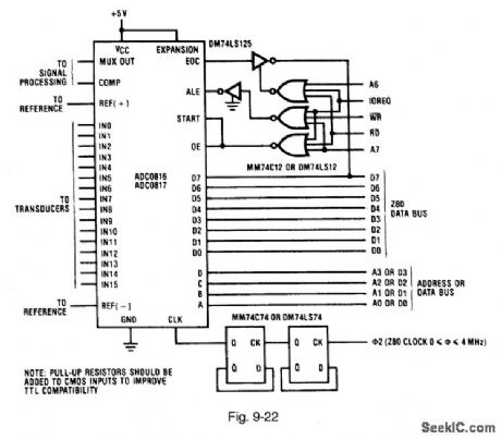
Figure 9-22 shows the ADC0816/17 connected to form a simple interface with classic Z80-type microprocessors. The 280, even though architecturally similar to the INS8080, uses slightly different control lines to perform I/O reads and writes. NOR gates are used to strobe the I/O functions. However, the Z80 has RD (read) and WR (write) strobes, which are gated with IOREQ (I/O request). START is connected to OE. This causes a new conversion to be started whenever the data bits are read. (Such a configuration can be useful if the converter is to be continually restarted upon completion of the previous conversion.) Address bit A6 is used to drive a strobe that placed EOC on the data bus to be read by the CPU. NATIONAL SEM[CONDUCTOR, APPLICATION NOTE 258, 1994, P. 607.
(View)
View full Circuit Diagram | Comments | Reading(1031)
8080_interface_with_partial_decoding
Published:2009/7/25 5:06:00 Author:Jessie
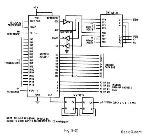
Figure 9-21 shows the ADC0816/17 connected with a DM74LS139 dual 2-4 decoder to form an 8080 interface with partial decoding. One half of the DM74SL139 is used to create read pulses, and the other half to create write pulses. The START and OE inputs are inverted to provide the correct pulse polarity. This interface partially decodes A6 and A7 to provide more I/O capabilities than the Fig. 9-20 circuit. The circuit in Fig. 9-21 also implements a simple polled-I/O structure. The EOC output is placed on the data bus by a tristate inverter when the inverter is enabled by a read pulse from the INS8080.
(View)
View full Circuit Diagram | Comments | Reading(621)
Simple_8080_interface
Published:2009/7/25 5:04:00 Author:Jessie
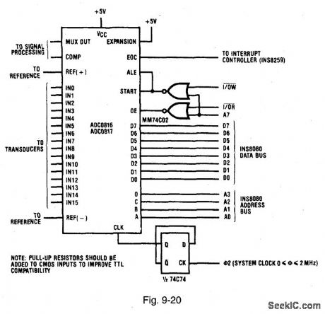
Figure 9-20 shows connections for interface between the ADC0816/17 and classic 8080-type microprocessors (INS8080/8224/8228). This interfacing is quite simple because the INS8080 CPU has separate I/O read (I/OR) and I/O write (I/OW) strobes (or separate I/O addressing). As a result, in this simple interface systems, little or no address decoding is required. Two NOR gates are used to gate the I/O strobes with the most-significant address bit A7. (The INS8080 has 8 bits of port address, yielding a maximum of four I/O ports if inputs A, B, C, and D are connected to the address bus.) An MM74C74 flip-flop is used as a divide-by-2 to generate a converter clock of 1 MHz. If the system clock is equal to or less than 1 MHz, the flip-flop can be omitted, Typical software for the Fig. 9-20 circuit first writes the channel address to the converter as a start signal. The two start pulses are sent to the ADCs to allow the comparator input to settle. After the second start pulse, the CPU can execute other program segments until the CPU is interrupted by EOC going high. Depending on interrupt structure, program control is then given to the interrupt handler, which reads the converter data. NATIONAL SEMICONDUCTOR, APPLICATION NOTE 258, 1994, P. 606. (View)
View full Circuit Diagram | Comments | Reading(1023)
Microprocessor_interface_considerations
Published:2009/7/25 5:02:00 Author:Jessie
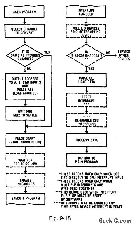
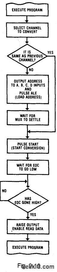
Figures 9-18 and 9-19 show flow charts for the interrupt-control and polled-I/O modes of ADC/microprocessor interface, respectively. Either interface can be used with the ADC0816/17, but the polled-I/O method usually requires fewer external components. With polled-I/O, the microprocessor (or CPU) periodically interrogates the ADC which looks like an I/O port to the CPU. With interrupt-control, the ADC appears as a memory and interrupts the microprocessor. From a simplified-design standpoint, the major concern is whether the EOC (end of conversion, Figi 9-3) should be polled by the microprocessor. Even though the actual timing of CPU read and write cycles varies, most microprocessors output the address and data (during write) onto the system buses. A certain time later, the read or write strobes go active for a specified time. The interface logic must detect the state of the address and data buses and initiate the action. For the ADC0816/17; these actions are: (1) load channel address, (2) start conversion, (3) detect EOC, and (4) read the resultant data. These functions are performed by decoding the read-write strobes, address, and data to form ALE and START pulses, then to detect EOC, and finally to read the data. NATIONAL SEMICONDUCTOR, APPLICATION NOTE 258, 1994, P. 605. (View)
View full Circuit Diagram | Comments | Reading(642)
ADC_with_sample_rand_hold_S_H
Published:2009/7/25 5:00:00 Author:Jessie
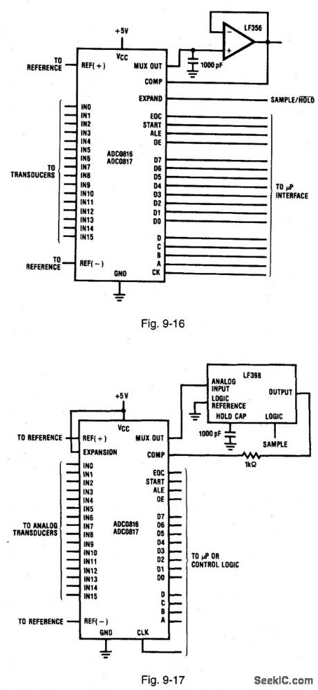
Figures 9116 and 9-17 show the ADC0816/17 connected for S/H operation. (The S/H function is the only major data-acquisition element not included in these ADCs.) If the input signals are fast moving, then an S/H should be used to quickly acquire the signal, then hold the signal while the ADCs convert it to a digital readout. This can be implemented by inserting an S/H function between the multiplexer output and the comparator input. In the simplest form, the multiplexer output is connected to the comparator input, with a capacitor connected to ground (similar to that shown in Fig. 9-16). The expansion-control pin is used as a sample-control input. When EXPAND is high, one switch is on and the capacitor voltage follows the input. When EXPAND is low, all switches are turned off and the capacitor holds the last value. However, this simple solution is not practical. The input bias to the comparator is about 2 μA (worst case, with a clock of 640 kHz). The droop (discharge rate) for a 1000-pF capacitor is about 2000 V/s (about 0.2-V per conversion). This is not practical. If a 0.01-μF capacitor is used instead, the rate is about 20 μV, which might work. However, the acquisition time would be about 100 μs, about the length of a conversion. The circuit of Fig. 9-16 eliminates the problem produced by the high comparator-input leakage. With the LF356 buffer connected between the multiplexer-output and comparator input pins, the leakage is reduced from 2 μA to about 100 nA. The droop-per-conversion is typically less than 1.0 μV per conversion (with the 1000-μF capacitor shown) and the acquisition time is about 20 ps (instead of the 100 ps). The circuit of Fig. 9-16 isolates the capacitor from both the multiplexer and comparator pins using an LF398 IC sample-and-hold. Acquisition time for the LF398 is a typical 4 μs to (0.1%), and droop rate is about 20 μV/conversion. Because the LF398 has its own S/H input, the expansion control of the ADC is free to be used in the normal manner. Use a hold capacitor with minimum dielectric absorption (polypropylene and polystyrene) for best results. NATIONAL SEMICONDUCTOR, APPLICATION NOTE 258, 1994, P. 603, 604. (View)
View full Circuit Diagram | Comments | Reading(660)
74 Series digital circuit of 74192,74L192 preset BCD decimal synchronous reversible counter(dual clock with clear)
Published:2011/8/1 0:45:00 Author:Lucas | Keyword: 74 Series , digital circuit , preset BCD decimal , synchronous reversible counterd, ual clock with clear


View full Circuit Diagram | Comments | Reading(3187)
CMOS_PROGRAMMABLE_DIVIDE_BY_N_COUNTER
Published:2009/6/28 21:53:00 Author:May

Circuit Notes
A single connection change permits division by any integer between 2 and 10. The RCA CD4017A Johnson decade counter is shown connected as a divide by 7 counter. The resistor is used to hold the reset line low. When the appropriate number is reached, that output and the reset line are driven high, resetting the counter. To divide by other integers, pin 15 should be connected to the desired output. For example, pin 1 for a divide by 5, or pin 7 for a divide by 3. The output of the divider appears on the 0 line. (View)
View full Circuit Diagram | Comments | Reading(1396)
ADC_with_at_icroprocessor_con_trolled_gain
Published:2009/7/25 4:58:00 Author:Jessie
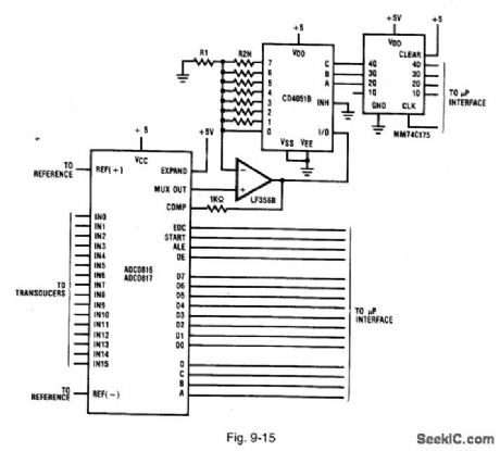
Figure 9-15 shows the ADC0816/17 connected for an external gain-control under supervision of a microprocessor. The CD4051 analog multiplexer is placed in the feedback loop of a simple noninverting op amp. The op-amp gain is controlled by selecting one of the CD4051 analog switches. This cuts a resistor in and out of the feedback loop. If the resistors (R2N) are of different value, different gains are realized. The gains are given by: Gain (AV) = 1 + (R2N/R1). A microprocessor (or some control logic) selects a gain by latching the channel address into a MM74C173. The LF356B output must not exceed the power supply. As a result, the op-amp gain must be reduced to a new level before a new channel is selected. The 1-kΩ resistor at the LF356B output helps protect the comparator inputs from accidental overvoltage (or undervoltage). The two back-biased diodes at the input to VCC and ground (1N914 or Schottky) offer further protection. NATIONAL SEMICONDUCTOR, APPLICATION NOTES 258, 1994, P. 602.
(View)
View full Circuit Diagram | Comments | Reading(871)
Buffering_circuits
Published:2009/7/25 4:53:00 Author:Jessie


Figures 9-13 and 9-14 show two typical buffering circuits for the ADCs. Three basic ranges of input signal levels can occur when ADCs are interfaces to the real world. These are as follows: (1) signals that exceed VCC or go below ground; (2) signals with input ranges less than VCC and ground, but are different from the reference range; and (3) signals that have an input range equal to the reference range. Each of these situations requires different buffering. In the last case (in which the signals are equal to the reference), no buffering is usually required, unless the source impedance of the input signal is very high. In this case, a buffer can be added between the multiplexer output and comparator input (Fig. 9-13). An op amp with high input impedance and low output impedance reduces input leakage (when one views the configuration from the multiplexer). If the input signal is within the supply range, but different from the reference range (or when the reference cannot be manipulated to conform to the full input range), the unity-gain buffer of Fig. 9-13 can be replaced with another op amp (as shown in the inset of Fig. 9-13). This type of amplifier provides gain or offset control to produce a full-scale range equal to the reference. When the input range exceeds VCC or goes below ground, the input signals must be level-shifted before the input can go to the multiplexer. There is a limit to such level shifting when the input voltage range is with 5 V, but outside the 0.5-V supply range. In this case, the supply for the entire chip can be shifted to the input range, and the digital-output signals can be level-shifted to the system 5-V supply. A typical example of level-shifting and buffering is the situation in which the bipolar inputs range from -2.5 V to +2.5 V. If the ADCs have the supply and reference provided (as shown in Fig. 9-14), then the ±2.5-V logic outputs can be shifted to 0-V and 5-V SEMICONDUCTOR, APPLICATION NOTE 258, 1994, P. 599.
(View)
View full Circuit Diagram | Comments | Reading(558)
74 Series digital circuit of 74190,74LS190 preset decimal reversible BCD counter(with mode control)
Published:2011/7/31 22:39:00 Author:Lucas | Keyword: 74 Series, digital circuit , preset decimal reversible , BCD counter, mode control


View full Circuit Diagram | Comments | Reading(3302)
Differential_16_channel_converter
Published:2009/7/25 4:49:00 Author:Jessie


Figure 9-12 shows the ADC0816/17 connected to provide for an ADC with 16 differential inputs. This circuit is a modification of the circuit in Fig. 9-10. The CD4051 addressing is changed, and a differential amplifier is added between the multiplexer outputs and the comparator input. The select logic for the CD4051 is modified to enable the switches so that they can be selected in parallel with the ADC. The output of the three multiplexers are connected to a differential amplifier, composed of two inverting amplifiers with gain and offset trimmers. A dual op-amp configuration of inverting amplifiers can be trimmed easily, and has less-stringent feedback-resistor matching requirements (than a single op amp). The transfer equation for the dual op amp shown is:
The propagation delay through the op amps is an important consideration. There must be sufficient time between the analog switch-selection and start-conversion to allow the analog signal at the comparator input to settle. Using the LF353 op amp shown, the delay is about 5 pus. The op-amp gain and offset controls are adjusted to provide the zero and full-scale digital-output readings for the analog-in-put range or span. NATIONAL SEMICONDUCTOR, APPLICATION NOTE 258, P. 598. (View)
View full Circuit Diagram | Comments | Reading(820)
| Pages:324/471 At 20321322323324325326327328329330331332333334335336337338339340Under 20 |
Circuit Categories
power supply circuit
Amplifier Circuit
Basic Circuit
LED and Light Circuit
Sensor Circuit
Signal Processing
Electrical Equipment Circuit
Control Circuit
Remote Control Circuit
A/D-D/A Converter Circuit
Audio Circuit
Measuring and Test Circuit
Communication Circuit
Computer-Related Circuit
555 Circuit
Automotive Circuit
Repairing Circuit