
Index 339
PLD_SYNCHRONIZES_ASYNCHRONOUS_INPUTS
Published:2009/6/24 3:26:00 Author:May

A programmable electrically erasable logic (PEEL) device can easily supply the synchronizing function. Digital systems often require synchronization of asynchronous inputs to avoid the potential metastability problems caused by setup-time violations. A common synchronization method uses two rippled 74LS72 D-type flip-flops.In this circuit, the asynchronous input feeds into the D input of the first flip-flop and its Q out-put feeds into the D of the second. Because the first flip-flop latches on the falling edge of the sys-tem clock, to avoid setup-time violations, the D input signal to the second flip-flop will be stabilized before the rising edge of the clock. Even experienced programmable-logic device designers often re-sort to such a TTL flip-flop circuit to handle the synchronization function, because of the architec-tural limitations of standard PLDs.A programmable elect;ically erasable logic (PEEL) device, such as the PEEL18CV8 from ICT, however, can easily supply the function. The user-programmable 12-configuration I/O macrocells in the device can internally feed back a signal before the output register. With this feedback arrange-ment, designing a two-stage input is simple.A gated-latch internally latches the asynchronous input on the falling edge of the system clock, generating signal Q1. ANDing the input with Q1 through the internal feedback path, eliminates a pos-sible hazard condition during the clock's high-to-low transition time. The latch then holds Q1 stable to ensure meeting the setup-time requirement of the subsequent D flip-flop, which, as before, regis-ters the signal on the next rising system clock edge.If by chance the input pulse width violates the set-up time of the gated latch, the clock's low time will give more time for settling. (View)
View full Circuit Diagram | Comments | Reading(0)
PLD_SYNCHRONIZES_ASYNCHRONOUS_INPUTS
Published:2009/6/24 3:26:00 Author:Jessie
A programmable electrically erasable logic (PEEL) device can easily supply the synchronizing function. Digital systems often require synchronization of asynchronous inputs to avoid the potential metastability problems caused by setup-time violations. A common synchronization method uses two rippled 74LS72 D-type flip-flops.In this circuit, the asynchronous input feeds into the D input of the first flip-flop and its Q out-put feeds into the D of the second. Because the first flip-flop latches on the falling edge of the sys-tem clock, to avoid setup-time violations, the D input signal to the second flip-flop will be stabilized before the rising edge of the clock. Even experienced programmable-logic device designers often re-sort to such a TTL flip-flop circuit to handle the synchronization function, because of the architec-tural limitations of standard PLDs.A programmable elect;ically erasable logic (PEEL) device, such as the PEEL18CV8 from ICT, however, can easily supply the function. The user-programmable 12-configuration I/O macrocells in the device can internally feed back a signal before the output register. With this feedback arrange-ment, designing a two-stage input is simple.A gated-latch internally latches the asynchronous input on the falling edge of the system clock, generating signal Q1. ANDing the input with Q1 through the internal feedback path, eliminates a pos-sible hazard condition during the clock's high-to-low transition time. The latch then holds Q1 stable to ensure meeting the setup-time requirement of the subsequent D flip-flop, which, as before, regis-ters the signal on the next rising system clock edge.If by chance the input pulse width violates the set-up time of the gated latch, the clock's low time will give more time for settling. (View)
View full Circuit Diagram | Comments | Reading(1646)
OPTICAL_PROXIMITY_DETECTOR
Published:2009/6/24 3:25:00 Author:Jessie
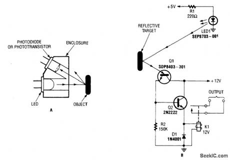
A reflector isolator (A) detects the presence of an object by bouncing light off of it. This tech-nique is useful in circuits that detect when an object is close enough to the sensor (B). (View)
View full Circuit Diagram | Comments | Reading(1389)
VOLTAGE_TRIPLER_FOR_RADONDETECTOR_IONIZATION_CHAMBER
Published:2009/6/24 3:22:00 Author:May

The voltage tripler charges the ionization chamber capacitor. It is powered from the 120-Vac line. Warning: Shock hazard exists. (View)
View full Circuit Diagram | Comments | Reading(1070)
ANALOG_SWITCH_CIRCUIT_1
Published:2009/6/24 3:24:00 Author:Jessie

View full Circuit Diagram | Comments | Reading(946)
SWITCH_ON_DELAY_CIRCUIT
Published:2009/6/24 3:19:00 Author:May

When S1 is tumed on, a very small current flows through the load. Almost the entire supply volt-age appears across the SCR. When C1 changes up to the firing voltage of Q1 (approximately the standoff ratio of Q1 times VS, usually 0.4 to 0.6 VS) through R1, Q1 fires, tuming on SCR1. This deliv-ers full voltage to load, minus SCR drop (about 1.2 V). Notice that load current must exceed SCR holding current. (View)
View full Circuit Diagram | Comments | Reading(729)
DIGITALLY_CONTROLLED_ONE_OF_FOUR_ANALOG_SWITCH
Published:2009/6/24 3:15:00 Author:May

View full Circuit Diagram | Comments | Reading(0)
POLARITY_PROTECTOR
Published:2009/6/24 3:13:00 Author:May

The use of a four-diode bridge guarantees correct polarity irrespective of input dc polarity. Remember that two diode drops (about 1.2 to 1.5 V) are lost from the input voltage using this circuit (View)
View full Circuit Diagram | Comments | Reading(768)
SHORT_CIRCUIT_PROTECTION_CIRCUIT
Published:2009/6/24 3:11:00 Author:May

When S1 is pressed, the coil of K1 is energized, closing its norrrtally open contacts. If the regulated dc input is between 1 and 24 V, that voltage feeds the base of Q1 through R1, turning on the transistor, and latching the relay. When that occurs, LED2 glows indicating that all is okay.If there is a short to ground at the circuit's output (i.e., in the device being powered), the voltage that feeds the base of Q1 goes to zero, turning off the transistor. Then, LED1 glows because K1 is de-energized to indicate the short circuit. (View)
View full Circuit Diagram | Comments | Reading(914)
NOVEL_LOUDSPEAKER_COUPLING_CIRCUIT
Published:2009/6/24 3:11:00 Author:May

The ground side of the speaker is con-nected to the junction of two equal high value capacitors (1000 μF is typical) across the sup-ply. The amplifier output voltage will be VS/2, and so will the voltage across C1 (if C1 and C2 are equal); so as the supply voltage builds up, the dc voltage across the speaker will remain zero, eliminating the switch-on surge. C1 and C2 will also provide supply smoothing. The circuit is shown with the LM380, but could be applied to any amplifier circuit, providing that the dc voltage at the output is half the supply voltage. (View)
View full Circuit Diagram | Comments | Reading(748)
8_DIGIT_100_MHz_FREQUENCY_PROBE
Published:2009/6/24 3:10:00 Author:May

Small enough to mount in a probe, this frequency counter circuit is good to 100 MHz. It operates from +5 to +15 Vdc. An 11C90 prescaler drives a 10-MHz counter chip (ICM7216B). Note the dotted line connecting R10 with pins 5 and 6 of IC2; that variable connection controls the decimal point and total count appearing on DSP1 and DSP2. The relative intensities and dura-tions of ON/OFF time for LED1 (green) and LED2 (red) give a rough indication of logic level and duty cycle. (View)
View full Circuit Diagram | Comments | Reading(7674)
OSCILLATOR_TRIGGERED_SWITCH
Published:2009/6/24 3:09:00 Author:May

In this circuit (the oscillator-triggered switch), the generated by an astable oscillator. (View)
View full Circuit Diagram | Comments | Reading(0)
LOW_OUTPUT_IMPEDANCE_MULTIPLEXER
Published:2009/6/24 3:08:00 Author:May

Both inputs are terminated in their characteristic impedance; 75Ω is typical for video applications. Because the output cables usually are terminated in their characteristic impedance, the gain is 0.5. Consequently, amplifiers U2A and U2B are configured in a gain of +2 to set the circuit gain at 1.R2 and R3 determine the amplifier gain; if a different gain is desired, R2 should be changed according to the equation G = (1 + R3/R2) R5, LCL1, and D1 make up an asymmetrical charge/discharge time circuit that configures U1 as a break-before-make switch to prevent both amplifiers from being ac-tive simultaneously. The multiplexer transition time is approximately 15μs with the component values shown. (View)
View full Circuit Diagram | Comments | Reading(0)
125_MHz_LOGIC_PROBE
Published:2009/6/24 3:06:00 Author:May

This logic probe features either high-low (LED) indication or latching operation. When S1 closed, the indication of a pulse is latched and the red LED1 stays on. Piezoelectric buzzer BZ1 used as a beeper to sound that a logic high is preset. (View)
View full Circuit Diagram | Comments | Reading(0)
ANALOG_SWITCH_CIRCUIT
Published:2009/6/24 3:05:00 Author:May

View full Circuit Diagram | Comments | Reading(680)
ANALOG_SWITCHED_INVERTER
Published:2009/6/24 3:05:00 Author:May

View full Circuit Diagram | Comments | Reading(524)
SIMPLE_RF_PROBE
Published:2009/6/24 3:05:00 Author:May

Your VTVM can measure peak voltage up to 200 MHz by using this probe. The maximum RF that can be measured is determined by the diode; with a 1N60, the probe is Iimited to 30 V. To increase the capacity, substitute a higher-voltage small-signal detector diode. House the circuit in a metal enclosure and use shielded wire. (View)
View full Circuit Diagram | Comments | Reading(1407)
SIMPLE_LOGIC_PROBE_WITH_ALPHANUMERIC_DISPLAY
Published:2009/6/24 3:03:00 Author:May

A logic probe also includes BCD decoder module. The red LED lights to indicate a logic high, and the green LED lights to indicate a logic low. This probe circuit will light a green (low) or red (high), and if desired, an alphanumeric display can be obtained with two 7-segment LED displays. (View)
View full Circuit Diagram | Comments | Reading(2043)
STEPPER_MOTOR_ENCODER_CIRCUIT
Published:2009/6/24 3:00:00 Author:May

This circuit translates shaft rotation and direction to a readout on an LED display. A stepper motor is used as an encoder. (View)
View full Circuit Diagram | Comments | Reading(0)
ADJUSTABLE_BIAS_REGULATOR
Published:2009/6/24 2:59:00 Author:May


If the wiper of R2 is set at N% rotation,the bias voltage Will be∶This method derives a bias voltage that tracks VBE of this bias transistor. If the bias transistor is thermally linked to the power stage, tracking over a wide temperature range will result. (View)
View full Circuit Diagram | Comments | Reading(0)
| Pages:339/471 At 20321322323324325326327328329330331332333334335336337338339340Under 20 |
Circuit Categories
power supply circuit
Amplifier Circuit
Basic Circuit
LED and Light Circuit
Sensor Circuit
Signal Processing
Electrical Equipment Circuit
Control Circuit
Remote Control Circuit
A/D-D/A Converter Circuit
Audio Circuit
Measuring and Test Circuit
Communication Circuit
Computer-Related Circuit
555 Circuit
Automotive Circuit
Repairing Circuit