
Index 323
74 Series digital circuit of 74273,74LS273 eight D flip-flop (with clear side)
Published:2011/8/1 1:42:00 Author:Lucas | Keyword: 74 Series , digital circuit , eight D flip-flop , (with clear side

Q0 = the output level before establishing the steady-state input conditions.
(View)
View full Circuit Diagram | Comments | Reading(2617)
74 Series digital circuit of 74LS266,74HC266 four 2 input XNOR(OC)
Published:2011/8/1 4:25:00 Author:Lucas | Keyword: 74 Series , digital circuit , four 2 input, XNOR, OC

View full Circuit Diagram | Comments | Reading(1801)
74 Series digital circuit of 74265 four complementary output circuit
Published:2011/8/1 1:40:00 Author:Lucas | Keyword: 74 Series , digital circuit, four complementary output

Units 1 and 4; Y=A,W=A; units 2 and 3; Y=AB, E=AB.
(View)
View full Circuit Diagram | Comments | Reading(564)
74 Series digital circuit of 74LS261 2 × 4-bit parallel binary multiplier
Published:2011/8/1 20:04:00 Author:Lucas | Keyword: 74 Series , digital circuit , 2 × 4-bit parallel , binary multiplier

5-bit is general 26ns; synchronization latch output; it can be extended to m-bit × n-bit application.
(View)
View full Circuit Diagram | Comments | Reading(1746)
74 Series digital circuit of 74LS257A,74F257 4-bit 2-to-1 data selector(tristate,in-phase)
Published:2011/7/25 4:27:00 Author:Lucas | Keyword: 74 Series, digital circuit , 4-bit , 2-to-1 data selector, tristate, in-phase

Three-state output is directly connected to the bus interface of the system, and 74LS257SA absorption current is 2 times larger than the 74LS257.
(View)
View full Circuit Diagram | Comments | Reading(966)
144_MHz_FOR_VSWR_BRlDGE
Published:2009/6/28 22:32:00 Author:May

Modulated signal source provides 10-mW CW output and 5mW modulated output at modulation frequency of 1000 Hz. Spurious and harmonic outputs are 40 dB below desired output. 72-MHzcrystal oscillator is followed by doubler stage. attenuation between generator and load. Use Oscillator runs continuously while doubler is regulated power supply or batteries.-J. flei-keyed whh simple ON/OFF square-wave keying, Freedom from load variations is obtained with double-tuned output filter providing up to 6-dB attenuation between generator and load, Use regulated power supply or batteries.-J.Reisert, Matching Techniques for VHF/UHF Antennas, Ham Radio, July 1976, p 50-56. (View)
View full Circuit Diagram | Comments | Reading(723)
74 Series digital circuit of 74LS256, 74F256 dual 4-bit addressable latch
Published:2011/8/1 4:32:00 Author:Lucas | Keyword: 74 Series , digital circuit , dual 4-bit , addressable latch

d = The H ot L data E before the conversion from low to high; q = the output state in the recent addressing or clearing cycle.
(View)
View full Circuit Diagram | Comments | Reading(709)
74 Series digital circuit of 74251,74LS251 8-to-1 data selector/driver(tristate)
Published:2011/8/1 4:23:00 Author:Lucas | Keyword: 74 Series, digital circuit , 8-to-1 data selector, driver, tristate

View full Circuit Diagram | Comments | Reading(1534)
74 Series digital circuit of 74LS253,74S253 dual 4 to 1 data selector (tristate)
Published:2011/8/1 1:38:00 Author:Lucas | Keyword: 74 Series , digital circuit , dual data selector, 4 to 1, tristate
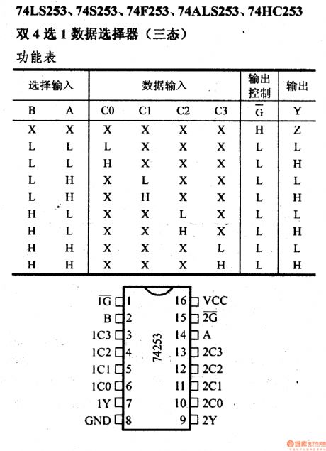
View full Circuit Diagram | Comments | Reading(783)
LOOP_PREAMP
Published:2009/6/28 22:31:00 Author:May

Loop for lower-frequency amateur bands is connected to gate of HEP802 FET and output to receiver istaken from FET source.C1 is two-gang variable capacitor from old broadcast radio, with stators in parallel to give 600 pF. Article gives loopdata for 40, 80, and 160 meters and for high end of broadcast band. For 40 and 80 meters, use 18-inch square loop with 2 tums spaced 1/4 inch. Ground lower end of 100K resistor to provide ground retum for FET.-K. Comell, Loop Antenna Receiving Aid, Ham Radio, May 1975, p 66-70. (View)
View full Circuit Diagram | Comments | Reading(933)
RF_NOISE_BRIDGE
Published:2009/6/28 22:30:00 Author:May

Improves accuracy and measurement range for impedance measurements from 3.5 to 30 MHz, particularly resistive and reactive components of high-frequency antennas. Accuracy is 3 ohms BMS. Wideband noise, generated in zener followed by threetransistor amplifier, is iniected into two legs of bridge in equal amounts by toroidal transformer having quadrifilar windings. With un known impedance connected and detectorlany communication receiver) set to desired frequency, reference impedances (250-ohm noninductive pot and 360-pF variable capacitor) are adjusted for deepest possible null. Value of unknown impedance is then equal to parallel combination of references. Article covers construction and calibration.-R. A. Hubbs and A. F.Doting, Improvements to the nx Noise Bridge, Ham Radio, Feb. 1977, p 10-20. (View)
View full Circuit Diagram | Comments | Reading(3941)
74 Series digital circuit of 74LS244,74F244 eight inverting buffer/line driver/ line receiver(three-state)
Published:2011/8/1 1:08:00 Author:Lucas | Keyword: 74 Series, digital circuit, eight inverting buffer, line driver, line receiver, three-state

When 1G, 2G are H, Y is in high resistance; when 1G, 2G are L, Y=A.
(View)
View full Circuit Diagram | Comments | Reading(3282)
74 Series digital circuit of 74LS241,74F241 eight inverting buffer/line driver/ line receiver(three-state)
Published:2011/8/1 1:06:00 Author:Lucas | Keyword: 74 Series , digital circuit , eight inverting buffer, line driver , line receiver, three-state

When 1G is H, 2G is L, Y is in high resistance; when 1G is L, and 2G is H, Y=A.
(View)
View full Circuit Diagram | Comments | Reading(855)
Q_MULTIPLIER_FOR_LOOP
Published:2009/6/28 22:20:00 Author:May

Improves performance of loop antenna on 40,80, and 160 meters. Feedback control is obtained with adjustable single-turn loop L3 coupled to L1, and receiver input is taken from L2. L3 is rotated within field.of L1 to adjust amount of regeneration, optimize circuit a, and make directional null more pronounced, Article gives loop con-struction details. Ground lower end of 100K ret sistorto provideground return for FET.-K, Cor-nell, Loop Antenna Receiving Aid, Ham Radio, May 1975, p 66-70. (View)
View full Circuit Diagram | Comments | Reading(2604)
74 Series digital circuit of 74S226 4-bit parallel latched bus transceiver
Published:2011/7/31 22:37:00 Author:Lucas | Keyword: 74 Series, digital circuit , 4-bit parallel latched, bus transceiver

The universal transceiver for system bus controller; double 4-bit transparent latch; one state output can directly drive the bus.
(View)
View full Circuit Diagram | Comments | Reading(782)
VSWR_BRIDGE
Published:2009/6/28 22:19:00 Author:May

Works well through 450 MHz to for measuring and matching VHF and UHF antennas. If identical load impedances are placed at J2 and J3, signals at opposite ends of R3 are equal and in phase and there is no output at J4. If impedances are different, output proportional to difference appears at J4 Impedance values can be from 25 to 100 ohms, although drcuit is designed for optimum performance at 50 ohms.-J. Reisert, Matching Techniques for VHF/UHF Antennas, Ham Radio, July 1976, p 50-56. (View)
View full Circuit Diagram | Comments | Reading(971)
Buffered_reference_used_as_a_power_supply
Published:2009/7/25 4:39:00 Author:Jessie

Figure 9-7 shows the ADC0816/17 used with a buffered reference. This method of buffering the reference provides higher current capabilities than the circuit of Fig. 9-6, and eliminates the IP term in the equation for resistor R. NATIONAL SEMICONDUCTOR, APPLICATION NOTE 258, 1994, P. 594. (View)
View full Circuit Diagram | Comments | Reading(578)
Using_the_referenc_as_the_supply
Published:2009/7/25 4:38:00 Author:Jessie


Figure 9-6 shows the ADC0816/17 connected with the external reference used asthe supply. The LM336-5.0 provides regulated 5-V for the ADC power andreference inputs as well as for the power input of other components in the system Of course an unregulated supply greater than 5 V is required for V+ Seriesresistor R is chosen so that the maximum current needed by the system is supplied and the LM336-5.0 is kept in regulation,The value of R is found by∶
where VS=unregulated supply voltage; VREF=reference voltage; ILAD =VREF/1 kΩ resistor ladder current; ITR =transducer currents IP=system power supply requirements; and IR = minimum reference current.NATIONAL SEMICONDUCTOR APPLICATION NOTE 258. 1994, P. 594.
(View)
View full Circuit Diagram | Comments | Reading(484)
74 Series digital circuit of 74198 8-bit shift register
Published:2011/7/29 1:26:00 Author:Lucas | Keyword: 74 Series , digital circuit , 8-bit shift register

Parallel storage; right shift(direction is from the QA to QH): left shift(direction is from the QH to QA); it forbids the clock.
a. .. h= the input of steady-state input level of A to H.
QAo,QBo, QGo, QHo=the input of steady-state input level of QAo,QBo, QGo, QHo.
QAn, QBn= the corresponding level ofQA, QB before the next jump of the clock.
(View)
View full Circuit Diagram | Comments | Reading(1768)
Absolute_conversion
Published:2009/7/25 4:34:00 Author:Jessie

Figure 9-5 shows the ADC0816/17 connected for simple absolute conversion. Absolute conversion refers to the use of transducers with which the output value is not related to another voltage. The absolute value of the output voltage is very important (in contrast to the output voltage of a ratiometric transducer). This implies that the reference must be accurate to determine the value of the absolute output of the transducer. A precise, adjustable reference is provided by an LM336-5.0 and the associated parts. Ratiometric transducers can also be used in this circuit, and in most of the following data-conversion circuits. However, the key point to remember is that accuracy of absolute conversion depends primarily on the accuracy of the reference voltage. With ratiometric systems (Fig. 9-4), accuracy is determined by the transducer characteristics. NATIONAL SEMICONDUCTOR, APPLICATION NOTE 259, 1994, P. 594. (View)
View full Circuit Diagram | Comments | Reading(598)
| Pages:323/471 At 20321322323324325326327328329330331332333334335336337338339340Under 20 |
Circuit Categories
power supply circuit
Amplifier Circuit
Basic Circuit
LED and Light Circuit
Sensor Circuit
Signal Processing
Electrical Equipment Circuit
Control Circuit
Remote Control Circuit
A/D-D/A Converter Circuit
Audio Circuit
Measuring and Test Circuit
Communication Circuit
Computer-Related Circuit
555 Circuit
Automotive Circuit
Repairing Circuit