
Index 331
DTL_TTL_CONTROLLED_BUFFERED_ANALOG_SWITCH
Published:2009/6/25 21:48:00 Author:May

This analog switch uses the 2N4860 JFET for its 25 ohm ron and low leakage. The LM102 serves as a voltage buffer. This circuit can be adapted to a dual trace oscilloscope chopper. The DS7800 monolithic IC provides adequate switch drive controlled by DTL/TTL logic levels. (View)
View full Circuit Diagram | Comments | Reading(0)
STEREO_BALANCER
Published:2009/6/25 21:46:00 Author:May

This circuit will allow you to set the gain of two stereo channels to the same level. The signal across the two channel-load resistors is sampled by resistors R2. (Values of these re-sistors will depend upon the power leveL) For most 20 milliampere LED, use approximately 2.5 K per watt. (For a 10-watt system use a 25,000 ohm resistor.) To set up, short the two inputs and connect them to one channel of a power amplifier. Apply a signal and adjust R3 until both LEDs glow at the same brightness level. The balancer is ready for use. Connect the inputs of the stereo balancer across the output of the power amplifier, and then turn up either the independent volume controls, or the balance control until both LEDs glow at the same level. To use this circuit in-line with loudspeakers, disconnect both R1s, and use the speakers as the load. (View)
View full Circuit Diagram | Comments | Reading(661)
DOUBLY_BALANCEDMIXER(BROADBAND_INPUTS,90_MHz_TUNED_OUTPUT)
Published:2009/6/25 21:33:00 Author:May

View full Circuit Diagram | Comments | Reading(456)
20_dB_VIDEO
Published:2009/6/25 21:33:00 Author:May

Simple circuit having gain of 20 dB provides 3-dB bandwidth of 20 MHz for CA3100 bipolar MOS opamp. Total noise referred to input is only 35μV RMS.- Circuit Ideas for RCA Linear ICs, RCA Solid State Di-vision, Somerville, NJ, 1977, p 12. (View)
View full Circuit Diagram | Comments | Reading(489)
ADJUSTABLE_TTL_CLOCK(MAINTAINS_50%DUTY_CYCLE)
Published:2009/6/25 21:25:00 Author:May

Symmetry of the square-wave output is maintained by connecting the right side of R2 through resistor R3 to the output of the third amplifier stage. This changes the charging cur-rent to the capacitors in proportion to the set-ting of frequency-adjusting potentiometer R2. Thus, a duty cycle of 50% is constant over the entire range of oscillation. The lower frequency limit is set by capacitor C2. With the components shown, the frequency of oscilla-tion can be varied by R2 from about 4 to 20 hertz. Other frequency ranges can be obtained by changing the values of C1 and R3, which control the upper limit of oscillation, or C2, which limits the low-frequency end. (View)
View full Circuit Diagram | Comments | Reading(663)
INVERSE_SCALER
Published:2009/6/25 21:25:00 Author:May

If a DAC is operated in the feedback loop of an operational amplifier,then the amplifiergain is inversely proportional to the input digital number or code to the DAC,The version giving scaling inversely proportional to posltive voltage is shown. (View)
View full Circuit Diagram | Comments | Reading(543)
VOLTAGE_CONTROL_RESISTOR
Published:2009/6/25 21:24:00 Author:May

View full Circuit Diagram | Comments | Reading(563)
TRIAC_TRIGGER
Published:2009/6/25 21:21:00 Author:May

View full Circuit Diagram | Comments | Reading(0)
FOUR_CHANNEL_DATA_ACQUlSITION_SYSTEM
Published:2009/6/25 21:20:00 Author:May

View full Circuit Diagram | Comments | Reading(0)
POSITIVE_EDGE_DIFFERENTIATOR
Published:2009/6/25 21:19:00 Author:May

View full Circuit Diagram | Comments | Reading(0)
STYLUS_ORGAN
Published:2009/6/25 21:18:00 Author:May

IC2 is an audio frequency oscillator. Its frequency is primarily controlled by the resistance between pins 2 and 7. RV4-11 control the oscillator frequency and by touching a stylus (connected via limiting resistor R5 to pin 2) to each preset, different notes can be played. IC1 is a low frequency oscillator (approximately 3-10Hz), the frequency of which is variable by RV1. The output of this oscillator is connected through depth control RV2 and limiting resistor R3 to the voltage control input of the audio frequency oscillator. Thus a vibrato effect occurs. (View)
View full Circuit Diagram | Comments | Reading(648)
NEGATIVE_EDGE_DIFFERENTIATOR
Published:2009/6/25 21:16:00 Author:May

View full Circuit Diagram | Comments | Reading(0)
LONG_DURATION_TIME_DELAY
Published:2009/6/25 21:14:00 Author:May

View full Circuit Diagram | Comments | Reading(0)
WIDEBAND_VARIABLE_GAIN
Published:2009/6/25 21:14:00 Author:May

FET selves as ourPur gain-controlled device in feedback loop of Optical Electronics 9906 opamp. Resistive T network has SD201 MOS transistor as ground leg, with resistor values dlosen so transistor is electrically dose to summing junction, automatically limiting total signal voltage. Resulting arrangement of voltage-controlled feedback and compensation gives variable-gain amplifier whh good linearity and constant wideband width for all gain Ievels.- Wideband Variable Gain Amplifier, Optical Electronics, Tucson, AZ, Application Tip 10277. (View)
View full Circuit Diagram | Comments | Reading(0)
SIREN_SPACE_WAR_PHASQR_GUN
Published:2009/6/25 21:13:00 Author:May

The one shot and decay functions could be added to make an ideal phasor gun sound. (View)
View full Circuit Diagram | Comments | Reading(1010)
STEREO_REVERB_ENHANCEMENT_SYSTEM
Published:2009/6/25 21:12:00 Author:May

The system can be used to synthesize a stereo effect from a monaural source such as AM radio or FM-mono broadcast, or it can be added to an existing stereo (or quad) system where it produces an exciting opening up special effect that is truly impressive. (View)
View full Circuit Diagram | Comments | Reading(975)
PROGRAMMABLE_BIRD_SOUNDS
Published:2009/6/25 21:11:00 Author:May

View full Circuit Diagram | Comments | Reading(558)
CAPACITANCE_MULTIPLIER
Published:2009/6/25 21:09:00 Author:May

This circuit can be used to simulate large capacitances using small value components. With the values shown and C = 10 μF, an effective capacitance of 10,000 μF was obtained. The Q available is limited by the effective series resistance. So R1 should be as large as practical (View)
View full Circuit Diagram | Comments | Reading(0)
DOOR_CHIMES_DELAY
Published:2009/6/25 21:06:00 Author:May
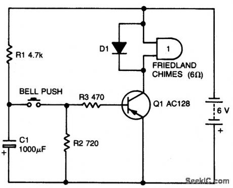
Circuit NotesWith values shown, this simple circuit will permit one operation every 10 seconds or so.Capacitor C1 charges through RI when the button is released. Making RI larger crease the delay. (View)
View full Circuit Diagram | Comments | Reading(0)
FOUR_CHANNEL_SYNTHESIZER
Published:2009/6/25 21:05:00 Author:May

This circuit will synthesize two rear chan-nels for quadraphonic sound when fed with a stereo signal. The rear output for the left chan-nel, is a combination of the left channel input 180 out of phase, added to a proportion of the right hand channel (also out of phase). The right hand rear output is obtained in a similar way. (View)
View full Circuit Diagram | Comments | Reading(0)
| Pages:331/471 At 20321322323324325326327328329330331332333334335336337338339340Under 20 |
Circuit Categories
power supply circuit
Amplifier Circuit
Basic Circuit
LED and Light Circuit
Sensor Circuit
Signal Processing
Electrical Equipment Circuit
Control Circuit
Remote Control Circuit
A/D-D/A Converter Circuit
Audio Circuit
Measuring and Test Circuit
Communication Circuit
Computer-Related Circuit
555 Circuit
Automotive Circuit
Repairing Circuit