
Index 334
MULTIPURPOSE_MODULE
Published:2009/6/24 23:41:00 Author:May

Flexible circuit using FET to drive bipolar transistor has -3 dB points at 100 Hz and 0.6 MHz. Components are noncritical and can be changed considerably in value to optimize gain, frequency response, power output, or power consumption. Load presented to FET is primarily input resistance of bipolar transistor, about 1000 ohms, which gives voltage gain of 4 for FET.-I. M Gottlieb, A New Look at Solid-State Amplifiers, Ham Radio, Feb. 1976, p 16-19. (View)
View full Circuit Diagram | Comments | Reading(0)
PARAPHASE_PHASE_INVERTER
Published:2009/6/24 23:34:00 Author:May

Uses 180° phase difference between source and drain out-puts of Siliconix Ut83 FET to convert AF input to push-pull output without transformer. Volt-age gain in each half of circuit is about 0.8. Frequency response referred to 1 kHz is flat within 3 dB from 50 Hz to 50 kHz, when using lmeg-ohm output load.-R. P. Turner, FET Circuits, Howard VV. Sams, Indianapolis, IN, 1977, 2nd Ed.,p 29-30. (View)
View full Circuit Diagram | Comments | Reading(0)
SUMMING_SCALING_VIDEO
Published:2009/6/24 23:31:00 Author:May

With Motorola MC1552G video amplifier connected as shown, summation of input signal currents is accom-plished at pin 4 through input resistors whose values arechosen to give desired scale factor.- A Wide Band Monolithic Video Amplifier, Mo-torola, Phoenix, AZ, 1973, AN-404, p 9. (View)
View full Circuit Diagram | Comments | Reading(498)
SINGLE_TRANSISTOR_CARRIER_CURRENT_RECEIVERTO_LINE_COUPLER
Published:2009/6/24 23:30:00 Author:May

View full Circuit Diagram | Comments | Reading(508)
AC_WITH_IMMUNITY_TO_LARGE_DC_OFFSET
Published:2009/6/24 23:29:00 Author:May

Designed to amplify from about 250 kHz down to Iow frequencies in presence of Iarge DC input offsets. Main NE540L ampllfier has gain of 101, while NE536T has DC gain of unity and forms part of Iow-pass network that applies DC input offset as common-mode voltage to inverting input of main amplifier.-A. Royston, Low Fre-quency A.C. Amplifier, Wireless World, May 1976, p 80. (View)
View full Circuit Diagram | Comments | Reading(626)
PHOTO_STROBE_SLAVE_TRIGGER
Published:2009/6/24 23:14:00 Author:May

The photo strobe slave trigger circuit uses a solar cell and an SCR to flash any strobe when you trigger your master strobe. The tiny solar cell produces a vet'y small voltage when light falls on its surface. (View)
View full Circuit Diagram | Comments | Reading(0)
TOUCH_CIRCUIT
Published:2009/6/24 23:10:00 Author:May

View full Circuit Diagram | Comments | Reading(0)
PHOTO_STROBE
Published:2009/6/24 23:00:00 Author:May
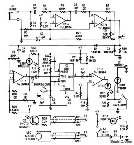
Sound or light sensors connected to J2 produce a voltage that is amplified by IC1-a and IC1-b. A positive trigger voltage that is developed by D1 and D3 and amplified by IC1-d, drives IC2 and IC1 to trigger SCR1. SCR1 is connected to a strobe. This device is handy for photographic purposes to take pictures of events that involve sound, such as impacts, etc. (View)
View full Circuit Diagram | Comments | Reading(0)
TOUCH_TRIGGERED_BISTABLE
Published:2009/6/24 22:59:00 Author:May

This circuit uses a 555 timer in the bista-ble mode. Touching T2 causes the output to go high; D2 conducts and Dl extinguishes. Touching T1 causes the output to go low; Dl conducts and D2 is cut off. The output from pin 3 can also be used to operate other circuits (e.g., a triac controlled lamp). In this case, the LEDs are useful for finding the touch terminals in the dark. C1 is not absolutely necessary but helps to prevent triggering from spurious pulses. (View)
View full Circuit Diagram | Comments | Reading(673)
OPTICAL_SCHMITT_TRIGGER
Published:2009/6/24 22:44:00 Author:May


This circuit shows a 555 with its trigger and threshold inputs connected together used to energize a relay when the light level on a photoconductive cell falls below a preset value. Circuit can be used in other applications where a high input impedance and low output impedance are required with the minimum component count. (View)
View full Circuit Diagram | Comments | Reading(992)
TIME_DELAY_FLASH_TRIGGER_CIRCUIT
Published:2009/6/24 22:43:00 Author:May

The circuit is built around a single 4093 quad 2-input NAND Schmitt trigger. Two gates from that quad package (U1-a and U1-b) are configured as a set-reset flip-flop. (View)
View full Circuit Diagram | Comments | Reading(1455)
PHASE_SHIFTER_WITH_EIGHT_OUTPUTS
Published:2009/6/24 22:39:00 Author:May

The circuit consists of eight cascaded identical cells, each cell being a dc-controlled active phase shifter. Because the dc control is common for all shifters, the circuit is adjusted by trimming RA so that the phase difference between V01 and Vi is zero. As a result, each shifter will introduce a phase difference of exactly π/r. The eight signals for PSK are available at the op amps' outputs.
Phase accuracy is acceptable for 1%-tolerance resistors and 5%-tolerance 100-nF capacitors. Also, the amplitude of Vi (which is a 1700-Hz sine wave), should not exceed 1 V. (View)
View full Circuit Diagram | Comments | Reading(722)
PHASE_SPLITTER_CIRCUIT
Published:2009/6/24 22:33:00 Author:May

This phase splitter uses a 2N2222 (or other general purpose npn transistor) to achieve outputs that are 180° out ofphase. (View)
View full Circuit Diagram | Comments | Reading(2462)
LONG_TAILED_PAIR_PHASE_SPLITTER
Published:2009/6/24 22:31:00 Author:May

The single-phase input produces out-of-phase outputs at the collectors of Q1 and Q2. (View)
View full Circuit Diagram | Comments | Reading(758)
PRECISION_PHOTODIODE_COMPARATOR_
Published:2009/6/24 22:31:00 Author:May

R1 sets the comparison level. At comparison, the photodiode has less than 5 mV across it, decreasing dark current by an order of magnitude. IC = LM 111/211/311. (View)
View full Circuit Diagram | Comments | Reading(725)
UNDERVOLTAGE_INDICATOR_FORBATTERY_OPERATED_EQUIPMENT
Published:2009/6/24 22:30:00 Author:May

Due to the low duty cycle of flashing LED, the average current drain is 1 mA or less. The NE555 will trigger the LED on when the moni-tored voltage falls to 12 volts. The ratio of R1 to R2 only needs to be changed if it is desired to change the voltage point at which the LED is triggered. (View)
View full Circuit Diagram | Comments | Reading(627)
PRECISION_BATTERY_VOLTAGE_MONITOR_FOR_HTS
Published:2009/6/24 22:29:00 Author:May

The precision voltage-monitor chip con-tains a temperature -compensated voltage ref-erence. R1 divides down the battery voltage to match the built-in reference voltage of IC1 (1.15 volts). When the voltage at pin 3 falls below 1.15 volts, pin 4 supplies a constant current of 7 mA to drive a small LED. About 0.2 LED) volt of hysteresis is added with R2. Without hysteresis, the LED could flicker on and off when the monitored voltage varies around the set point, as might be the case on voice peaks during receive. (View)
View full Circuit Diagram | Comments | Reading(592)
OPTICAL_COMMUNICATION_SYSTEM
Published:2009/6/24 22:28:00 Author:May

The simple modulator stage will accommodate most common LEDs. By adjusting the potentiometer, the bias ofthe transistor is varied until the LED is at its half output point.Then, audio will cause it to vary above and below this point. The purpose of R1 is to limit the current through the LED to a safe level and the purpose of the 10 ohm resistor is to allow a portion of the modulating signal to be observed on a scope. (View)
View full Circuit Diagram | Comments | Reading(0)
ULTRASONIC_PEST_REPELLER
Published:2009/6/24 22:28:00 Author:May


This circuit uses two transistors and one IC (555 timer IC) to produce a pulsating ultrasonic frequency. Transistors Q1 and Q2 are connected in a direct-coupled oscillator. The frequency of that oscillator is set by capacitor C1. The oscillator output is taken from the emitter of Q2 to pin 7 of IC1. Transistor Q1 is an npn transistor, and Q2 is a pnp transistor. The signal of pin 7 on IC1 causes the output signal appearing ot) pin 3 to be modulated or varied by the audio frequency developed by Q1 and Q2. The IC itself is connected as a stable multivibrator with a frequency that is determined by C3. Capacitor C3 sets the basic frequency to be well above the human hearing range (ultrasonic). The combined modulated ultrasonic frequency appears on pin 3 of IC1, where it is coupled by capacitor C4 to the piezoelectric transducer. (View)
View full Circuit Diagram | Comments | Reading(0)
EQUIPMENT_ON_REMINDER
Published:2009/6/24 22:26:00 Author:May

Due to the low duty cycle of flashing LED, the average current drain is 1 mA or less. (View)
View full Circuit Diagram | Comments | Reading(538)
| Pages:334/471 At 20321322323324325326327328329330331332333334335336337338339340Under 20 |
Circuit Categories
power supply circuit
Amplifier Circuit
Basic Circuit
LED and Light Circuit
Sensor Circuit
Signal Processing
Electrical Equipment Circuit
Control Circuit
Remote Control Circuit
A/D-D/A Converter Circuit
Audio Circuit
Measuring and Test Circuit
Communication Circuit
Computer-Related Circuit
555 Circuit
Automotive Circuit
Repairing Circuit