Basic Circuit
Simple_8080_interface
Published:2009/7/25 5:04:00 Author:Jessie | From:SeekIC

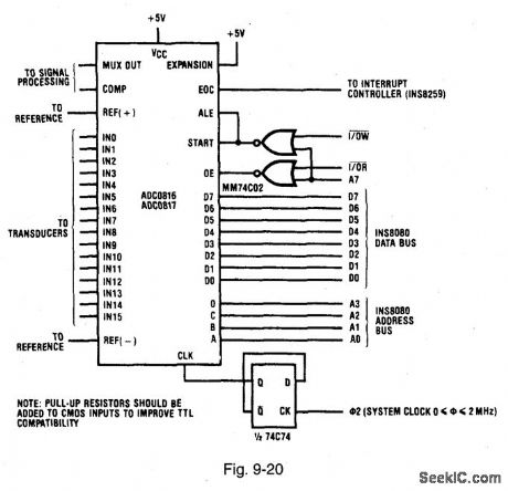
Figure 9-20 shows connections for interface between the ADC0816/17 and classic 8080-type microprocessors (INS8080/8224/8228). This interfacing is quite simple because the INS8080 CPU has separate I/O read (I/OR) and I/O write (I/OW) strobes (or separate I/O addressing). As a result, in this simple interface systems, little or no address decoding is required. Two NOR gates are used to gate the I/O strobes with the most-significant address bit A7. (The INS8080 has 8 bits of port address, yielding a maximum of four I/O ports if inputs A, B, C, and D are connected to the address bus.) An MM74C74 flip-flop is used as a divide-by-2 to generate a converter clock of 1 MHz. If the system clock is equal to or less than 1 MHz, the flip-flop can be omitted, Typical software for the Fig. 9-20 circuit first writes the channel address to the converter as a start signal. The two start pulses are sent to the ADCs to allow the comparator input to settle. After the second start pulse, the CPU can execute other program segments until the CPU is interrupted by EOC going high. Depending on interrupt structure, program control is then given to the interrupt handler, which reads the converter data. NATIONAL SEMICONDUCTOR, APPLICATION NOTE 258, 1994, P. 606.
Reprinted Url Of This Article:
http://www.seekic.com/circuit_diagram/Basic_Circuit/Simple_8080_interface.html
Print this Page | Comments | Reading(3)

Article Categories
power supply circuit
Amplifier Circuit
Basic Circuit
LED and Light Circuit
Sensor Circuit
Signal Processing
Electrical Equipment Circuit
Control Circuit
Remote Control Circuit
A/D-D/A Converter Circuit
Audio Circuit
Measuring and Test Circuit
Communication Circuit
Computer-Related Circuit
555 Circuit
Automotive Circuit
Repairing Circuit
Code: