
Automotive Circuit
Index 23
Mazda 96PROBE(2.5L) charging system circuit
Published:2011/8/23 22:24:00 Author: | Keyword: Mazda, 96PROBE, charging system circuit
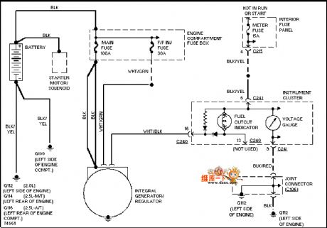
The Mazda 96PROBE(2.5L) charging system circuit is as shown in the figure:
(View)
View full Circuit Diagram | Comments | Reading(901)
Mazda 96PROBE 2-speed windscreen wiper washer circuit
Published:2011/8/23 22:24:00 Author: | Keyword: Mazda, 2-speed, windscreen wiper, washer circuit
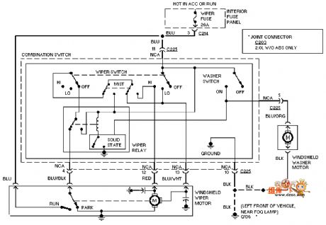
The Mazda 96PROBE 2-speed windscreen wiper washer circuit is as shown in the figure:
(View)
View full Circuit Diagram | Comments | Reading(947)
Mazda 96PROBE iron distribution circuit
Published:2011/8/23 22:24:00 Author: | Keyword: Mazda, iron distribution circuit
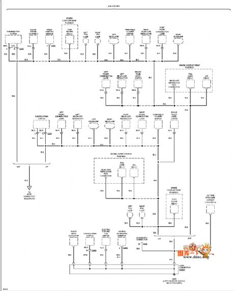
The Mazda 96PROBE iron distribution circuit is as shown in the figure:
(View)
View full Circuit Diagram | Comments | Reading(531)
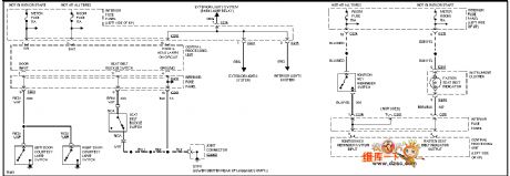
Mazda 96PROBE remote control door lock circuit
Published:2011/8/23 22:25:00 Author: | Keyword: Mazda, remote control, door lock circuit

The Mazda 96PROBE remote control door lock circuit is as shown in the figure:
(View)
View full Circuit Diagram | Comments | Reading(1676)
Mazda 96PROBE alarm system circuit
Published:2011/8/14 8:25:00 Author:Christina | Keyword: Mazda, alarm system circuit
Mazda 96PROBE alarm system circuit:
(View)
View full Circuit Diagram | Comments | Reading(518)
Mazda 96PROBE demisting precipitator circuit
Published:2011/8/14 8:26:00 Author:Christina | Keyword: Mazda, demisting precipitator
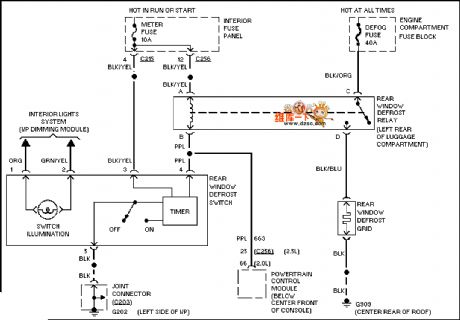
The Mazda 96PROBE demisting precipitator circuit is as shown in the figure:
(View)
View full Circuit Diagram | Comments | Reading(501)
Mazda 96PROBE dashboard circuit
Published:2011/8/14 8:27:00 Author:Christina | Keyword: Mazda, dashboard circuit
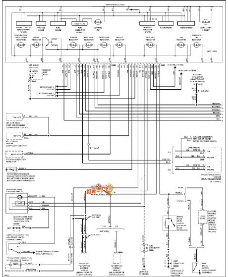
Mazda 96PROBE dashboard circuit is as shown in the figure:
(View)
View full Circuit Diagram | Comments | Reading(634)
The regulator: DC-DC circuit, power supply monitor pin and its main features AN8000M
Published:2011/8/23 23:44:00 Author:Seven | Keyword: DC-DC circuit, power supply, monitor pin
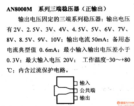
The 3-terminal stabilizer (forward output) of AN8000M series This is a 3-terminal stabilizer with a fixed output voltage; the output voltage can be 2V, 2.5V, 3V,4V, 4.5V, 5V, 6V, 7V, 8V, 9V and 10V; the output current 50mA; the typical value of the standby state current is 0.6mA; the minimum input-output voltage difference is lower than 0.3V; the max input voltage is 20V; the working temperature is -30~+80⁰C; it contains the over-current protection circuit.
(View)
View full Circuit Diagram | Comments | Reading(505)
The regulator: DC-DC circuit, power supply monitor pin and its main features CW117M/217M/317M
Published:2011/8/24 0:36:00 Author:Seven | Keyword: DC-DC circuit, power supply, monitor pin
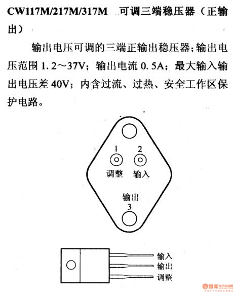
CW117M/217M/317M--the adjustable 3-terminal stabilizer (positive output)This is an adjustable 3-terminal stabilizer whose output voltage is adjustable; the output voltage range is 1.2~37V; the output current is 0.5A; the max input-output voltage difference is 40V; it contains the over-current, over-heat and secure working area protection circuit.
(View)
View full Circuit Diagram | Comments | Reading(585)
The regulator: DC-DC circuit, power supply monitor pin and its main features CW117L/217L/317L
Published:2011/8/24 0:37:00 Author:Seven | Keyword: DC-DC circuit, power supply, monitor pin
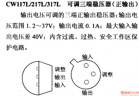
CW117L/217L/317L--the adjustable 3-terminal stabilizer (positive output) This is an adjustable 3-terminal stabilizer whose output voltage is adjustable; the output voltage range is 1.2~37V; the output current is 0.1A; the max input-output voltage difference is 40V; it contains the over-current, over-heat and secure working area protection circuit.
(View)
View full Circuit Diagram | Comments | Reading(576)
The regulator: DC-DC circuit, power supply monitor pin and its main features BA6121
Published:2011/8/24 0:15:00 Author:Seven | Keyword: DC-DC circuit, power supply, monitor pin
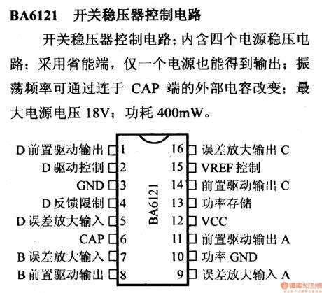
The switch stabilizer control circuit of BA6121This is a switch stabilizer control circuit which contains 4 power supply stabilizer circuits. It is adopted with the energy-saving terminals, by which even only one power supply can generate output; the oscillating frequency can be changed by the external capacitor linking to CAP terminal; the max power supply voltage is 18V; the power consumption is 400mW.
(View)
View full Circuit Diagram | Comments | Reading(606)
78PGA--The regulator: DC-DC circuit, power supply monitor pin and its main features
Published:2011/8/23 22:21:00 Author:Seven | Keyword: DC-DC circuit, power supply, monitor pin
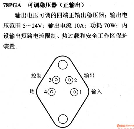
78PGA adjustable stabilizer (positive output) This is a 4-terminal positive stabilizer whose output voltage is adjustable; its output voltage range is 5~24V; its output current is 10A; its power consumption 70W; it contains the output short circuit current limitation, heat over-load and secure working area protection device.
(View)
View full Circuit Diagram | Comments | Reading(576)
The regulator: DC-DC circuit, power supply monitor pin and its main features AN6530/6531
Published:2011/8/23 22:22:00 Author:Seven | Keyword: DC-DC circuit, power supply, monitor pin
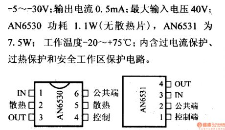
AN6530/6531 the adjustable regulator (forward output) This is a 4-terminal stabilizer whose output voltage is stable; the output voltage range is -5~-30V; output current is 0.5mA; the maximum input voltage is 40V; AN6530 power consumption is 1.1W (without radiators); it contains over-current protection, over-heat protection and secure working area protection circuit. (View)
View full Circuit Diagram | Comments | Reading(517)
The regulator: DC-DC circuit, power supply monitor pin and its main features AN5902S
Published:2011/8/23 22:21:00 Author:Seven | Keyword: DC-DC circuit, power supply, monitor pin
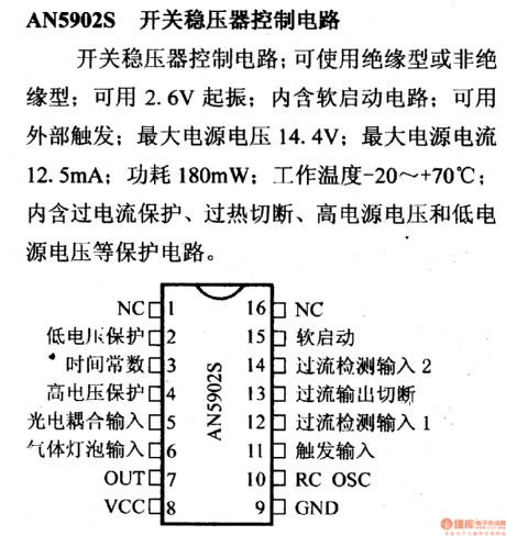
AN5902S--the switch stabilizer control circuit This is a switch stabilizer control circuit; either the insulated or non-insulated can be used; it can be oscillated with a 2.6V voltage; it contains the soft starting circuit;it can be triggered externally; the max power supply voltage is 14.4V; the max power supply current is 12.5mA; the working temperature is -20~+70⁰C; it contains the over-voltage, over-current, high power supply voltage, low power supply voltage and other protection circuits.
(View)
View full Circuit Diagram | Comments | Reading(487)
The regulator: DC-DC circuit, power supply monitor pin and its main features 79N00
Published:2011/8/23 22:21:00 Author:Seven | Keyword: DC-DC circuit, power supply, monitor pin

The 3-terminal stabilizer (negative output) of 79N00 series This is a 3-terminal positive stabilizer with fixed output voltage; its max output current 300mA; the max input voltage of 79N04~79N18 IS -35v; the max input voltage of 79N20 and 79N24 is -40V; the power consumption is 8W; its working temperature is -29~+80⁰C; it contains the over-current limitation, over-heat protection and secure working area limitation circuit. The types of similar products are AN79N00 and μPC79N00H.
(View)
View full Circuit Diagram | Comments | Reading(662)
The main features of the amplifier pin signal--μA702 wide frequency band general computer
Published:2011/8/23 22:48:00 Author:Seven | Keyword: main features, pin signal, wide frequency band, general computer
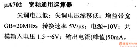
μA702 wide frequency band general computer Low maladjustment voltage; low maladjustment voltage drift; the band width of the gain is GB=20MHz; converting speed rate is 5V/μs; power supply is ±10V; common mode input voltage is 1.5V~6V; output current (peak value) is 50mA.
(View)
View full Circuit Diagram | Comments | Reading(753)
The main features of the amplifier pin signal--μA715 high computing amplifier
Published:2011/8/23 22:17:00 Author:Seven | Keyword: main features, high computing amplifier, pin signal
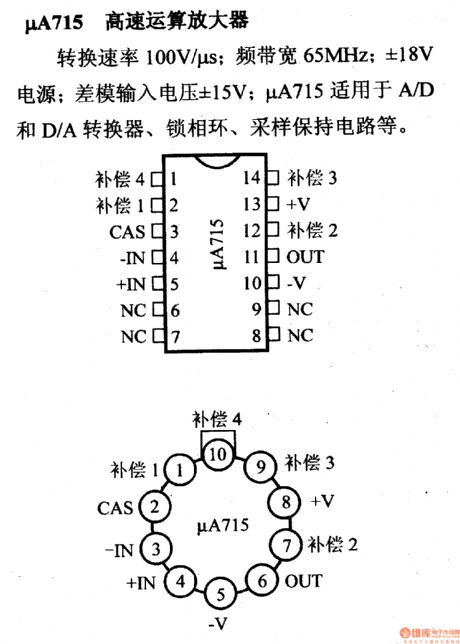
μA715 high computing amplifier Converting speed rate is 100V/μs; frequency band width is 65±MHz; ±18V power supply; difference mode input voltage is ±15V; μA715 is suitable for A/D and D/A converter, PLL, sampling maintenance circuit and so on.
(View)
View full Circuit Diagram | Comments | Reading(621)
The main features of the amplifier pin signal--μA739/749 dual low-noise computing amplifier
Published:2011/8/23 22:17:00 Author:Seven | Keyword: main features, pin signal, computing amplifier
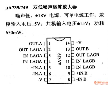
μA739/749 dual low-noise computing amplifier
Low noise, ±08V power supply, single power supply available; difference mode input voltage is ±5V; common mode input voltage is ±15V; power consumption is 650mA.
(View)
View full Circuit Diagram | Comments | Reading(1003)
The main features of the amplifier pin signal--μA771 general JFET input computing amplifier
Published:2011/8/23 22:18:00 Author:Seven | Keyword: main features, amplifier, JFET
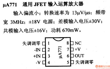
μA771 general JFET input computing amplifier Low input bias current; converting speed rate is 13μV/μs; frequency band width is 3MHz; ±18V power supply; difference mode input voltage is ±30V; common mode input voltage is ±16V; power consumption is 670mA.
(View)
View full Circuit Diagram | Comments | Reading(695)
The main features of the amplifier pin signal--μA772 dual general JFET input computing amplifier
Published:2011/8/23 22:18:00 Author:Seven | Keyword: main features, pin signal, JFET, input computing amplifier
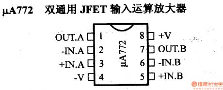
μA772 dual general JFET input computing amplifier
(View)
View full Circuit Diagram | Comments | Reading(698)
| Pages:23/164 At 202122232425262728293031323334353637383940Under 20 |
Circuit Categories
power supply circuit
Amplifier Circuit
Basic Circuit
LED and Light Circuit
Sensor Circuit
Signal Processing
Electrical Equipment Circuit
Control Circuit
Remote Control Circuit
A/D-D/A Converter Circuit
Audio Circuit
Measuring and Test Circuit
Communication Circuit
Computer-Related Circuit
555 Circuit
Automotive Circuit
Repairing Circuit