
Amplifier Circuit
Index 158
MONOSTABLE_MULTIVIBRATOR_I
Published:2009/6/23 22:26:00 Author:Jessie
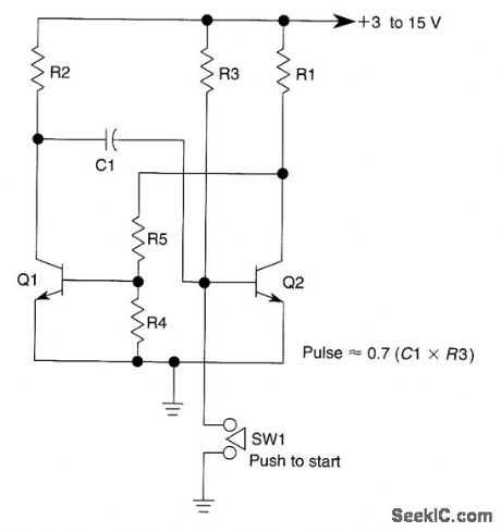
This circuit is activated when SW1 is pushed to ground the base of transistor Q2. The pulse rate is approximately equal to 0.7(R3×C1). (View)
View full Circuit Diagram | Comments | Reading(552)
VIDEO_AMPLIFIER
Published:2009/6/23 4:03:00 Author:May

View full Circuit Diagram | Comments | Reading(1498)
OP_AMP_LINEAR_SAWTOOTH_GENERATOR
Published:2009/6/23 4:34:00 Author:May

Q1 is connected in a simple constant-current generator circuit. The value of Q1's emitter resistor sets the constant-current level flowing from the transistor's collector to the charging capacitor, C1.One op amp of an LM324.quad op-amp IC, UI-a, is connected in a voltage-follower circuit. The input impedance on the voltage follower is very high and offers little or no load on the charging cir-cuit. The follower's output is connected to the input of UI-b, which is configured as a voltage com-parator. The comparator's other input is tied to a voltage-divider setting the input level to about 8 V.The output of UI-b at pin 7 switches high when the voltage at its positive input, pin 5, goes above 8 V. That turns on Q2, discharging C1. The sawtooth cycle is repeated over and over as long as power is applied to the circuit.The sawtooth's frequency is determined by the value of C1 and the charging current supplied to that capacitor. As the charging current increases, the frequency also increases, andvice versa, To in-crease the generator's frequency range, decrease the value of C1, and to lower the frequency, in-crease the value of C1. The output is about 3 to5V. (View)
View full Circuit Diagram | Comments | Reading(0)
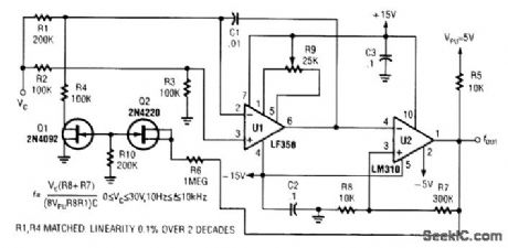
10_Hz_TO_10_kHz_3_DECADE_VCO
Published:2009/6/23 4:37:00 Author:Jessie
View full Circuit Diagram | Comments | Reading(1191)
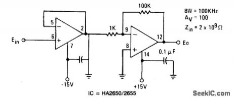
HIGH_IMPEDANCE,HIGH_GAIN,HIGH_FREQUENCY_INVERTING_AMP
Published:2009/6/23 3:29:00 Author:May
View full Circuit Diagram | Comments | Reading(455)
NONINVERTING_AMPLIFIER
Published:2009/6/23 3:28:00 Author:May
View full Circuit Diagram | Comments | Reading(1093)
PREAMPLIFIER_AND_HIGH_TO_LOW_IMPEDANCE_CONVERTER
Published:2009/6/23 3:28:00 Author:May
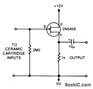
This circuit matches the very high impedance of ceramic cartridges, unity gain, and low impedance output. By loading the cartridge with a 2M2 input resistance, the cartridge characteristics are such as to quite closely compensate for the RIAA recording curve. The output from this,preamp may be fed to a level pot for mixing. (View)
View full Circuit Diagram | Comments | Reading(2086)
MOISTURE_DETECTOR
Published:2009/6/23 3:55:00 Author:Jessie
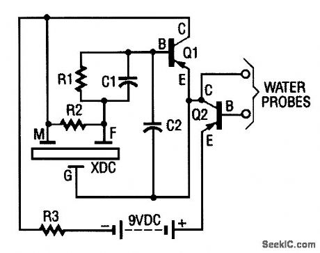
The moisture detector uses two transistors and a piezoelectric transducer to sound an alarm tone when water is present. Transistor Q1 forms a crystal-controlled oscillator, using a portion of piezoelectric transducer XDC-which contains two piezoelectric crystal regions-as the crystal. The transducer has three separate leads, One lead goes to each of the crystals, and the third lead is com-rnon to both.
The smaller internal crystal region sets the frequency of operation and the larger element is driven by Q1 (when it is biased on ) to provide the loud tone output. To turn the pnp transistor Q1 (used as an oscillator) on pnp transistor Q2 (used here as a switch) must be on. To turn it on with the biasing that is normally connected, you would only need to connect a resistor from the collector of Q2 to the base, which gives the base a negative (-) bias. The resistor used is the water that is to be detected. That turns Q2 on, which, in turn, turns on Q1. The result when water touches the probe is that the transducer emits a loud sound. (View)
View full Circuit Diagram | Comments | Reading(1)
PRECISION_AMPLIFIER
Published:2009/6/23 3:26:00 Author:May
View full Circuit Diagram | Comments | Reading(404)
GROUND_LOOP_PREVENTER
Published:2009/6/23 3:32:00 Author:Jessie

Ground loops are caused by improper grounding. Ground-loop voltages can interfere with test rrteasurements because the voltages in a ground loop can be larger than the signals you're trying to measure. To prevent ground loops, use two wire plugs to provide the line power to the test instru-ments and a separate wire to bring the input grounds of the instruments to a common ground. (View)
View full Circuit Diagram | Comments | Reading(1092)
HIGH_INPUT_IMPEDANCE_HIGH_OUTPUT_CURRENT_VOLTAGE_FOLLOWER
Published:2009/6/23 3:25:00 Author:May
View full Circuit Diagram | Comments | Reading(643)
BABY_MONITOR
Published:2009/6/23 3:31:00 Author:Jessie

Transmitter operation. Operating power for the transmitter circuit is derived directly from the ac line. The dc power to operate the circuit is generated in two stages, one for an RE power-amplifier stage, and the second for the remainder of the circuit.
The ac line voltage is applied to D1 , which half-wave rectifies the ac input . The resulting dc voltage (approximately 30V under load) is fed across an RC filter (comprised of R1 and C1) and used to operate amplifier, Q1. The second stage of the power supply (composed of LED1, R2, D2, D3, C2, and C3, which forms a regulated +13.6-V, center-tapped supply) feeds the remainder of the circuit. LED1 is connected in series with R2 and is used as a visual power-on indicator for the transmitter.
An electret microphone element (MIC1) is used as the pick-up. The output of the microphone is ac coupled through C5 to UI-a (a noninverting op amp with a gain of about 100). The output of U1-a at pin 1 is ac coupled through C4 to the noninverting input of UI-b (which provides an additional gain of 48) at pin 5. The output of UI-b at pin 7 is then fed through D4 and RIO, and across R11 and C6 to the inverting input of UI-c which is biased to a positive voltage that is set by SENSITIVITY-control R19. This represents a threshold voltage at which the output of UI-c switches from high to low.
During standby, the output of UI-c at pin 8 is held at about 12 V when the voltage developed across C6 is less than the bias-voltage setting at pin 10. When a sound of sufficient intensity and du-ration is detected, the voltage at pin 9 of UI-c exceeds the threshold level (set by R19), causing UI-c's output at pin 8 at go low. That low is applied to pin 2 of U2 (a 555 oscillator/timer configured as a monostable multivibrator). This causes the output of U2 to go high for about one second, as de-termined by the time constant of R12 and C7. The output of U2 at pin 3 is applied to pin 4 of U3 (a second 555 oscillator/timer that is conftgured for astable operation, with a frequency of about 125 kHz). That causes U3 to oscillate, producing a near square-wave output that is used to drive Q1 into conduction. The output of Q1 is applied across a parallel-tuned circuit composed a T1's primary and C8. The tuned circuit, in turn, reshapes the 125-kHz signal, causing a sine-wave-like signal to appear across both the primary and the secondary of Tl.
The signal appearing at T1's secondary (about 1 or 2 V peak-to-peak) is impressed across the ac power line, and is then distributed throughout the building without affecting other electrical appli-ances connected to the line. Transient suppressor D7 is included in the circuit to help protect Q1 from voltage spikes that might appear across the power line and be coupled to the circuit through T1.
Receiver operation. Power for the receiver, as with the transmitter, is derived from a tradi-tional half-wave rectifier (D5). The resulting dc voltage is regulated to 27 V by D6 and R20, and is then filtered by C11 to provide a relatively clean, dc power source for the circuit. A light-emitting diode, LED2, connected in sGries with R20 provides a visual indication that the circuit is powered and ready to receive a signal.
The 125-kHz signal is plucked from the ac line and coupled through R21 and C12 to a parallel-tuned LO circuit, consisting of C13 and L1. That LO circuit passes 125-kHz signals while attenuating all others. The 125-kHz signal is fed through C14 to the base of Q2 (which is configured as a high-gain linear amplifier), which boosts the relatively low amplitude of the 125-kHz signal. The RE out-put of Q2 is ac coupled to the base of Q3 through C15. Transistor Q3 acts as both an amplifier and detector. Because there is no bias voltage applied to the base of Q3, it remains cut off until driven by the amplified 125-kHz signal. When Q3 is forward biased, its collector voltage rises.
Capacitor C16, connected across Q3's collector resistor, filters the 125-kHz signal so that it is essentially dc. When the voltage at the collector of Q3 rises, Q4 is driven into conduction. That causes current to flow into piezo buzzer BZ1, producing a distinctive audio tone that alerts anyone within earshot that the baby needs attention. (View)
View full Circuit Diagram | Comments | Reading(2519)
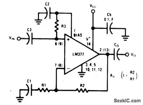
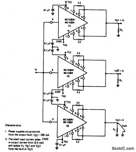
AUDIO_DISTRIBUTION_AMPLIFIER
Published:2009/6/23 3:24:00 Author:May

View full Circuit Diagram | Comments | Reading(0)
INVERTING_AMPLIFIER
Published:2009/6/23 3:31:00 Author:Jessie

View full Circuit Diagram | Comments | Reading(1111)
LOG_RATIO_AMPLIFIER
Published:2009/6/23 3:30:00 Author:Jessie
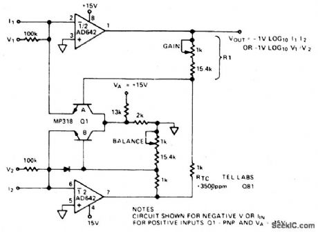
View full Circuit Diagram | Comments | Reading(746)
SIGNAL_DISTRIBUTION_AMPLIFIER
Published:2009/6/23 3:23:00 Author:May
View full Circuit Diagram | Comments | Reading(488)
DIODELESS_PEAK_HOLD_CIRCUIT
Published:2009/6/23 3:38:00 Author:Jessie

The input pulse is fed into the sample-and-hold amplifier (an inexpensive AD582), as well as the comparator U3. The SHA's output also is fed into the comparator. If the input pulse is higher in am-plitude than the SHA's output, the comparator output goes low and the 4538 one-shot produces a l0-ps pulse that is fed back to cause the SHA to sample and then hold the voltage. Subsequent input voltages that are less than the held value won't cause the one-shot to fire again.Gates U4A and U4B are used to inhibit the sampling when necessary. Gates U4C and U4D, at the one-shot's output, can force the AD 582 into the sample mode. This feature is useful to reset the output to zero by forcing a sample when the input to the AD582 is zero. The polarity of the peak-hold circuit can be easily changed from positive-to-negative peak hold by reversing the inputs of the comparator. (View)
View full Circuit Diagram | Comments | Reading(2160)
ACID_RAIN_MONITOR
Published:2009/6/23 3:37:00 Author:Jessie

The drain-to-source resistance of Q1 varies depending on the acidity of the sample presented to Q1's gate circuit. That variable resistance varies the current flowing through the bridge; that current is proportional to pH. (View)
View full Circuit Diagram | Comments | Reading(1942)
FET_OP_AMP_MICROPHONE_MIXER
Published:2009/6/23 3:03:00 Author:May

View full Circuit Diagram | Comments | Reading(609)
PIEZOELECTRIC_BUFFER
Published:2009/6/23 3:00:00 Author:May
This circuit will serve as a buffer for experiments with Kynar film, a piezoelecffic material, or with piezo devices. (View)
View full Circuit Diagram | Comments | Reading(1698)
| Pages:158/250 At 20141142143144145146147148149150151152153154155156157158159160Under 20 |
Circuit Categories
power supply circuit
Amplifier Circuit
Basic Circuit
LED and Light Circuit
Sensor Circuit
Signal Processing
Electrical Equipment Circuit
Control Circuit
Remote Control Circuit
A/D-D/A Converter Circuit
Audio Circuit
Measuring and Test Circuit
Communication Circuit
Computer-Related Circuit
555 Circuit
Automotive Circuit
Repairing Circuit