
Amplifier Circuit
Index 157
10_W_POWER_AMPLIFIER
Published:2009/6/24 3:07:00 Author:Jessie
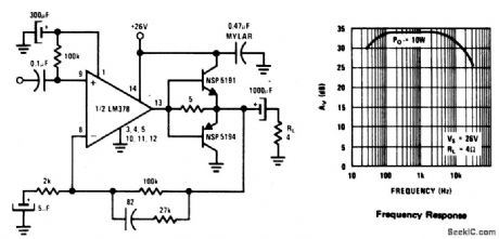
View full Circuit Diagram | Comments | Reading(1188)
12_W_LOW-DISTORTION_POWER_AMPLIFIER
Published:2009/6/24 3:06:00 Author:Jessie
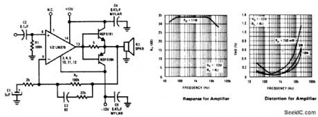
View full Circuit Diagram | Comments | Reading(594)
LOW_COST_20_W_AUDIO_AMPLIFIER
Published:2009/6/24 2:59:00 Author:May

This simple inexpensive audio amplifier can be constructed using a couple of TO-220 monolithic Darlington transistors for the push-pull output stage. Frequency response is flat within t dB from 30 Hz to 200 kHz with typical harmonic distortion below 0.2%. The amplifier requires only 1.2 Vrms, for a full 20 W output into an 8 ohm load. Only one other transistor is needed, the TO-92 low-noise high-gain 2N5961 (Q1), to provide voltage gain for driving the output Darlingtons. Its base (point B) is the tie point for ac and dc feedback as well as for the signal input. Input resistance is 10 K. The center voltage at point A is set by adjusting resistor R4. A bootstrap circuit boosts the collector supply voltage of Q1 (point C) to ensure sufficient drive voltage for 6)2. This also provides constant voltage across R7, which therefore acts as a current source and, together with diodes Dl-D3, reduces low-signal crossover distortion. (View)
View full Circuit Diagram | Comments | Reading(2385)
NONINVERTING_AMPLIFIER_USING_SINGLE_SUPPLY
Published:2009/6/24 3:02:00 Author:Jessie
View full Circuit Diagram | Comments | Reading(618)
FAST_COMPOSITE_AMPLIFIER
Published:2009/6/24 3:01:00 Author:Jessie
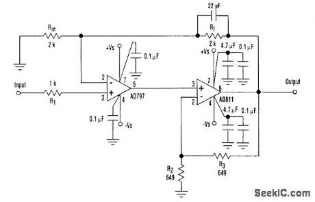
An ultra-low-noise, low-distortion op amp-the AD797-is combined with the AD811 op amp, which offers a high bandwidth and a 100-mA output drive capability. The composite-amplifier circuit serves quite well when driving high resolution ADC's and ATE systems.
The fast AD811 operates at twice the gain of the AD797 so that the slower amplifier need only slew one-half of the total output swing. Using the component values shown, the circuit is capable of better than -90 dB THD with a ±5-V, 500-kHz output signal. If a 100-kHz sine-wave input is used, the circuit will drive a 600-Ω load to a level of 7 V rms with less than -109 dB THD, as well as a 10-kΩ load at less than -117 dB THD.
The device can be modified to supply an overall gain of 5 by changing both the Rf/Rin ratio and R3/R2 ratio to 4: 1. This raises the gains of AD811 and the total circuit while maintaining the AD797 at unity gain. If only the Rf/Rin ratio is changed, the circuit might become unstable. In contrast, if only the R3/R2 ratio is varied, the AD797 will then operate at gain. Subsequently, the circuit will have a lower overall bandwidth. R1 should be equal to the parallel combination of Rin and Rf. (View)
View full Circuit Diagram | Comments | Reading(3380)
BRIDGE_AMPLIFIER
Published:2009/6/24 3:01:00 Author:Jessie
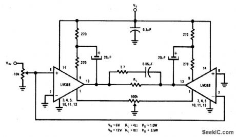
This circuit is for low voltage applications requiring high power outputs. Output power levels of 1.0 W into 4 ohm from 6 V and 3.5 V into 8 ohm from 12 V are typical. Coupling capacitors are not necessary since the output dc levels will be within a few tenths o f a volt of each other. Where critical matching is required the 500 K potentiometer is added and adjusted for zero dc current flow through the load. (View)
View full Circuit Diagram | Comments | Reading(1377)
75_WATT_AUDIO_AMPLIFIER_WITH_LOAD_LINE_PROTECTION
Published:2009/6/24 3:00:00 Author:Jessie

View full Circuit Diagram | Comments | Reading(1007)
AMPLIFIED_NOISE_LIMITER_FOR_SW_RECEIVERS
Published:2009/6/24 2:44:00 Author:May
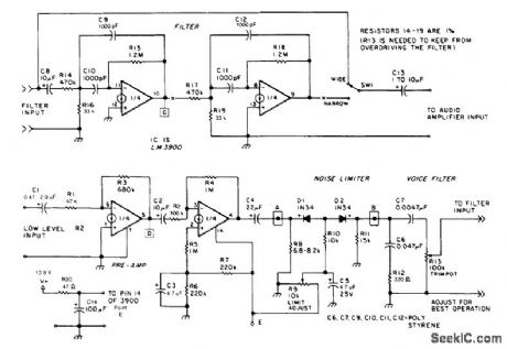
The noise limiter circuit has a preamplifier clipper, and a switchable audio bandpass filter. Audio levels in the 5- to 50-mV range are amplified in a preamp to several volts p-p, fed to a clipper, voice band filter, then to a narrow band active filter which can be switched in and out of the circuit. (View)
View full Circuit Diagram | Comments | Reading(2800)
MIXER_PREAMPLIFIER_WITH_TONE_CONTROL
Published:2009/6/24 2:17:00 Author:May

General purpose preamplifier/mixer accepts up to four inputs, has a gain of 1600, and provides bass and treble controls that can be varied ±10 dB at 100 kHz resectively. IC1 and IC2 = LM301A. (View)
View full Circuit Diagram | Comments | Reading(985)
DIGITALLY_CONTROLLED_AMPLIFIER_ATTENUATOR
Published:2009/6/24 2:02:00 Author:May
View full Circuit Diagram | Comments | Reading(506)
CXA1642P Song Elimination Integrated Circuit
Published:2011/7/22 21:52:00 Author:Michel | Keyword: Elimination Integrated Circuit
CXAI642P is karaoke songs elimination integrated circuit produced by SONY and it is mainly used in TV
acoustics and audio etc.
First,CXAI642P Typical Application Circuit
CXAI642P intergrated block typical application circuit is shown as the picture 1.Picture 1:CXAI642P Intergrated Block Typical Application Circuit
Second,CXAI642P Pins Functions and DataIntegrated circuit CXAI642P uses 8 feet DIP encapsulation structure, and its integrated circuit pins functions and data are shown as table 1.
Table 1:CXAI642P Pins Functions and Data
Third,Ciruit Work ProcessR accompaniment and singing enters CXA1642P feet ① after the capacitance coupling.L accompaniment and singing enters CXA1642P feet ⑧ after the capacitance coupling.And the accompanying song is eliminated after it is solved.
(View)
View full Circuit Diagram | Comments | Reading(472)
10A Power Amplifier Circuit
Published:2011/7/13 20:16:00 Author:Sue | Keyword: Power, Amplifier
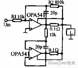
The 10A power amplifier uses two high power operational amplifiers OPA541 which can acquire continuous output of 10A. Theupper one is phase reversal amplifier while theunder one is connected with unit gain circuit. For the load, these two amplifiers are output-parallel. The 0.1Ω resistor limits the output current into 5A. The 20pF capacitor is used to prevent high frequency self-excitation.
(View)
View full Circuit Diagram | Comments | Reading(670)
231 Dual amplifier circuit diagram
Published:2011/7/28 3:27:00 Author:Ecco | Keyword: Dual amplifier
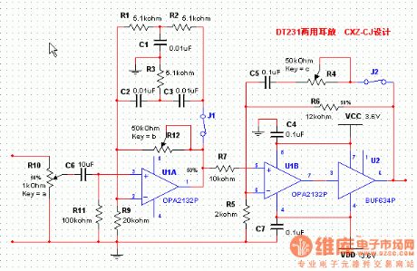
R4 is a low frequency upgrading adjustable resistor replaced by the 12K fixed resistor, and then, it will gradually increase under 100Hz, reach 5-6dB (2 times) under 50Hz, no upgrade above 100Hz. R12 is the If adjustable resistor and replaced by 30K fixed resistors, it makes 2.5-4.5KHz frequency increase, and the band upgrade approximately 6 dB (2 times). If you feel harsh, it needs to add RC, double T decreases. For a fixed resistor, in addition to enhance the band, the circuit overall voltage amplification factor is 3 times, it is enough to push down the headset.J1, J2 are the linkage switch, you can choose generic options or DT231-specific amp. Due toit upgrade little, Q value is not high, the relative frequency change is not great. Due to circuit change little, Q value is not high, the relative frequency change is not great.
(View)
View full Circuit Diagram | Comments | Reading(564)
FREE_RUNNING_MULTIVIBRATOR_USING_OP_AMP
Published:2009/6/23 22:36:00 Author:Jessie
View full Circuit Diagram | Comments | Reading(705)
LINEARAMAMPLITUDE_MODULATOR
Published:2009/6/23 5:01:00 Author:May
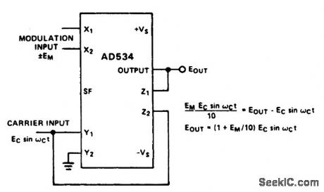
This is a very simple amplitude modulator. It makes use of the Z2 terminal to add the carrier directly to the output, thus bypassing the multi-plier for zero modulation input. It has the advan-tage of allowing operation from a differential modulation input. (View)
View full Circuit Diagram | Comments | Reading(658)
FLIP_FLOP_OR_BISTABLE_MULTIVIBRATOR_WITH_PUSHBUTTON_TRIGGERING
Published:2009/6/23 22:35:00 Author:Jessie
View full Circuit Diagram | Comments | Reading(594)
ASTABLE_MULTIVIBRATOR_Ⅱ
Published:2009/6/23 22:33:00 Author:Jessie

An astable multivibrator based on the 555 is shown. Freq is approximately 975 Hz as determined by the values of RB and C. (View)
View full Circuit Diagram | Comments | Reading(534)
MONOSTABLE_MULTIVIBRATOR_II
Published:2009/6/23 22:31:00 Author:Jessie
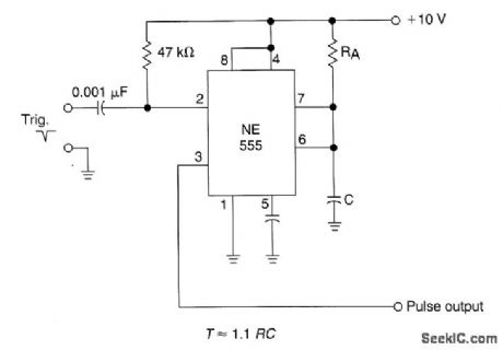
The time constant of RAXC deterrrtines the period of the monostable multivibrator. A negative pulse at pin 2 of the 555 starts the cycle. (View)
View full Circuit Diagram | Comments | Reading(736)
IMPROVED_CMOS_MULTIVIBRATOR
Published:2009/6/23 22:23:00 Author:Jessie
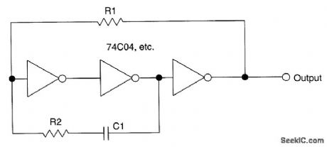
This circuit uses a protective resistor R2 in conjunction with feedback resistor R1. Together, they form a voltage divider to reduce the input voltage amplitude for IC1-a so that the protective diodes never conduct. This improves temperature and voltage stability of the multivibrator. (View)
View full Circuit Diagram | Comments | Reading(714)
VERY_LOW_FREQUENCY_MULTIVIBRATOR
Published:2009/6/23 22:25:00 Author:Jessie
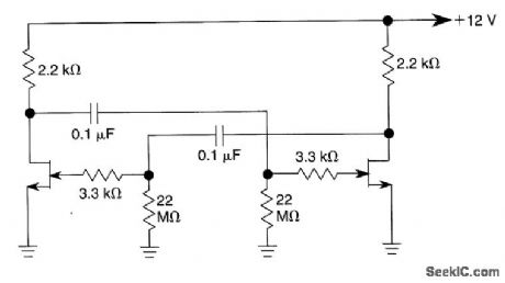
The use of JFETs permits, high resistance and long time constants in this very low frequency multivibrator. The values shown are for 0.15 Hz operation. (View)
View full Circuit Diagram | Comments | Reading(892)
| Pages:157/250 At 20141142143144145146147148149150151152153154155156157158159160Under 20 |
Circuit Categories
power supply circuit
Amplifier Circuit
Basic Circuit
LED and Light Circuit
Sensor Circuit
Signal Processing
Electrical Equipment Circuit
Control Circuit
Remote Control Circuit
A/D-D/A Converter Circuit
Audio Circuit
Measuring and Test Circuit
Communication Circuit
Computer-Related Circuit
555 Circuit
Automotive Circuit
Repairing Circuit