
Amplifier Circuit
Index 156
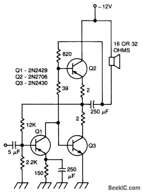
PHONNO_AMPLIFIER
Published:2009/6/24 3:18:00 Author:May
View full Circuit Diagram | Comments | Reading(500)
INVERTING_POWER_AMPLIFIER
Published:2009/6/24 3:14:00 Author:May

View full Circuit Diagram | Comments | Reading(1233)
NONINVERTING_POWER_AMPLIFIER
Published:2009/6/24 3:13:00 Author:May
View full Circuit Diagram | Comments | Reading(830)
LOW_NOISE_AND_DRIFT_COMPOSITE_AMP
Published:2009/6/24 3:13:00 Author:May
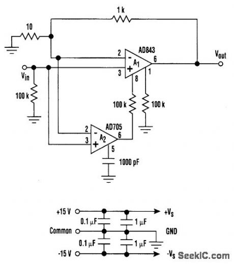
This circuit offers the best of both worlds, It can be combined with a low input offset voltage and drift without degrading the overall system's dynamic performance. Compared to a standalone FETinput operational amplifier, the composite amplifier circuit exhibits a 20-fold improvement in voltage offset and drift.
In this circuit arrangement, A1 is a highspeed FET input op amp with a closed-loop gain of 100 (the source impedance was arbitrarily chosen to be 100 kΩ). A2 is a SuperBeta bipolar input op amp. It has good dc characteristics, biFET-level input bias current, and low noise. A2 monitdrs the voltage at the input of Al and injects current to Al's null pins. This forces A1 to have the input properties of a bipolar amplifier while maintaining its bandwidth and low-inputbias-current noise. (View)
View full Circuit Diagram | Comments | Reading(721)
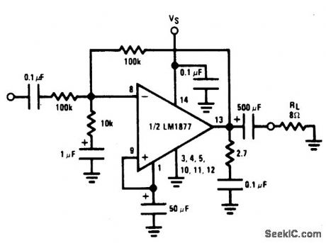
NONINVERTING_AC_POWER_AMPLIFIER
Published:2009/6/24 3:12:00 Author:May
View full Circuit Diagram | Comments | Reading(557)
470_mW_COMPLEMENTARY_SYMMETRY_AUDIO_AMPLIFIER
Published:2009/6/24 3:10:00 Author:May
This circuit has less than 2% distortion and is flat within 3 dB from 15 Hz to 130 kHz. (View)
View full Circuit Diagram | Comments | Reading(677)
PHONOGRAPH_AMPLIFIERCERAMIC_CARTRIDGE
Published:2009/6/24 3:18:00 Author:Jessie
View full Circuit Diagram | Comments | Reading(616)
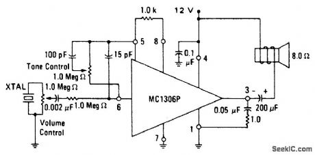
PHONO_AMPLIFIER_WITH_“COMMON_MODE”VOLUME_AND_TONE_CONTROL
Published:2009/6/24 3:17:00 Author:Jessie
View full Circuit Diagram | Comments | Reading(420)
4_W_BRIDGE_AMPLIFIER
Published:2009/6/24 3:15:00 Author:Jessie
View full Circuit Diagram | Comments | Reading(420)
HIGH_GBW_OP_AMP
Published:2009/6/24 3:15:00 Author:Jessie
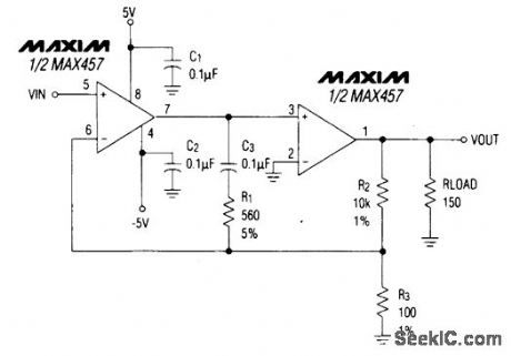
You can build a composite amplifier featuring high gain, wide bandwidth, and good dc accuracy by cascading the sections of a dual video amplifier and adding two appropriate phase-compensation components. The op amp drives a 150-Ω load and provides a closed-loop gain of 40 dB. (View)
View full Circuit Diagram | Comments | Reading(868)
OP_AMP_AND_ANALOG_SWITCH_RON_COMPENSATOR
Published:2009/6/24 3:08:00 Author:May
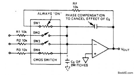
This switch is in series with feedback resistor to compensate gain. (View)
View full Circuit Diagram | Comments | Reading(1088)
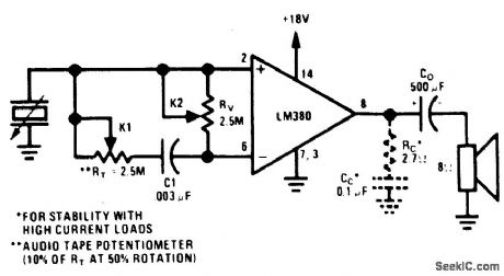
6_W,8’OHM_OUTPUT_TRANSFORMERLESS_AMPLIFIER
Published:2009/6/24 3:04:00 Author:May
View full Circuit Diagram | Comments | Reading(505)
VARIABLE_GAIN_OP_AMP_CIRCUIT
Published:2009/6/24 3:10:00 Author:Jessie
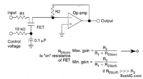
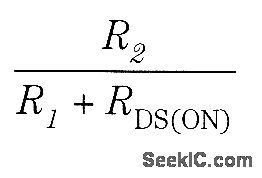
A JFET acts as a variable attenuator for this op amp. Maximum gain is: (View)
View full Circuit Diagram | Comments | Reading(906)
NONLINEAR_OPERATIONAL_AMPLIFIER_WITH_TEMPERATURE_COMPENSATED_BREAKPOINTS
Published:2009/6/24 3:04:00 Author:May
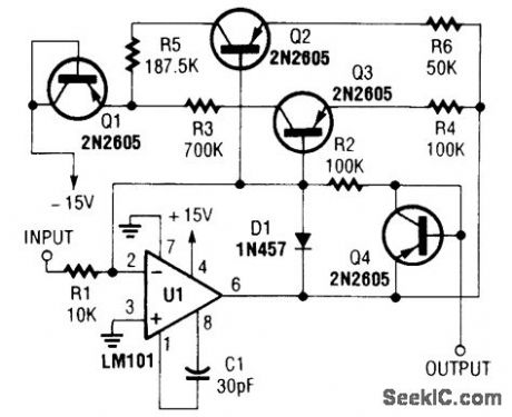
Using resistor and transistor feedback elements, this operational amplifier circuit can be used as a nonlinear amplifier. R4 and R6 can be varied to change breakpoints, as required. (View)
View full Circuit Diagram | Comments | Reading(1144)
NONINVERTING_AMPLIFIER_USING_SPLIT_SUPPLY
Published:2009/6/24 3:03:00 Author:May
View full Circuit Diagram | Comments | Reading(551)
CURRENT_PROBE_AMPLIFIER
Published:2009/6/24 3:02:00 Author:May
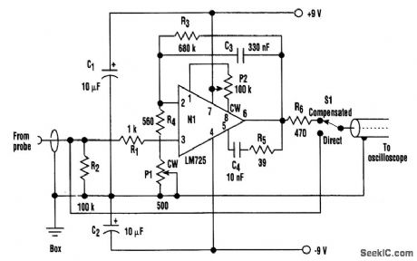
A clamp-on current probe, such as the Tektronix P6021, is a useful means of displaying current waveforms on an oscilloscope. A less-expensive and simple alternative is shown in the figure.The more sensitive range on the P6021 is 2 mA/mV, but it has a roll-off of 6-dB per octave below 450 Hz. The purpose of the compensator is to counteract the low-frequency attenuation, which is achieved by means of C3 and R4 + P1 in the feedback around op amp N1. It's important that the latter is a low-noise type, such as the LM725 shown in the figure. On top of that, it's necessary at some point to limit the increasing gain with decreasing frequency; otherwise, amplifier noise and drive will overcome the signal. The values shown for C3 and R3 give a lower limit of less than 1 Hz.A test square wave of ±1 mA is fed to the current probe so that P1 can be adjusted for minimum droop or overshoot in the output waveform. It's vital that the sliding core on the probe is fully closed. At high frequencies, the response begins to fall off at 100 kHz. Therefore, for most waveforms, switch S1 is moved to direct, above a fundamental frequency of, for example, 10 kHz.This circuit's current consumption is quite low, and it can be battery powered. If a mains power supply is built-in, it must be well screened to prevent hum problems. (View)
View full Circuit Diagram | Comments | Reading(1617)
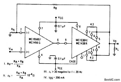
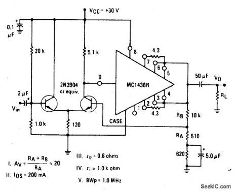
POWER_OP_AMP
Published:2009/6/24 3:08:00 Author:Jessie
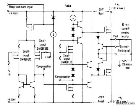
This circuit from Apex Microtechnology can deliver 180 V p-p@90 kHz into a 4-Ωload.The PA04 can deliver 400-W RMS into an 8-Ω load with low THD at frequencies beyond 20 kHz. (View)
View full Circuit Diagram | Comments | Reading(721)
AM_RADIO_POWER_AMPLIFIER
Published:2009/6/24 3:08:00 Author:Jessie

View full Circuit Diagram | Comments | Reading(514)
STEREO_AMPLIFIER_WITH_Av=200
Published:2009/6/24 3:08:00 Author:Jessie
View full Circuit Diagram | Comments | Reading(602)
pH_PROBE_AMPLIFIER
Published:2009/6/24 3:07:00 Author:Jessie

The low-noise precision FET op-amp AD795 has around 1014-Ω common-mode impedance, lowoffset voltage (250 μVmax) and L13 μVC drift make this device ideal for low-voltage measurements from high-impedance sources. (View)
View full Circuit Diagram | Comments | Reading(700)
| Pages:156/250 At 20141142143144145146147148149150151152153154155156157158159160Under 20 |
Circuit Categories
power supply circuit
Amplifier Circuit
Basic Circuit
LED and Light Circuit
Sensor Circuit
Signal Processing
Electrical Equipment Circuit
Control Circuit
Remote Control Circuit
A/D-D/A Converter Circuit
Audio Circuit
Measuring and Test Circuit
Communication Circuit
Computer-Related Circuit
555 Circuit
Automotive Circuit
Repairing Circuit