
Amplifier Circuit
Index 151
CMOS_PIEZO_DRIVER_USING_4049
Published:2009/6/24 23:41:00 Author:May

This circuit uses a 4049 IC to drive a 2N2222 switching transistor The transistor drives crysbal 1 a ptezo transducer. (View)
View full Circuit Diagram | Comments | Reading(2382)
CMOS_PIEZO_DRIVER
Published:2009/6/24 23:39:00 Author:May

A CMOS-gate and transistor buffer can be used as an effective driver for a piezoelectric transducer. (View)
View full Circuit Diagram | Comments | Reading(1103)
500_kHz_TO_500_MHz
Published:2009/6/24 23:34:00 Author:May
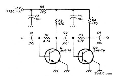
Two-stage general-pur-pose wideband small-signal amplifier provides nearly 14-dB gain at 150 MHz when inserted in 50-ohm transmission line with no tuned circuits at input or output. Noise figure with optimum source resistance is about 3 dB at 150 MHz. Am-plifier is capaeitively coupled common-emitter cascade. Capacitors make low-frequency gain begin dropping off below about 2 MHz. Increas-ing all capacitors to 0.01μF will lowerfrequency response to about 200 kHz.-R. Rhea, General Purpose Wideband RF Amplifier, Ham Radio, April 1975, p 58-61. (View)
View full Circuit Diagram | Comments | Reading(972)
IMPEDANCE_CONVERTER
Published:2009/6/24 23:42:00 Author:Jessie

Used to match 10-megohrninputimpedanceto 50-ohm transmission Iine or 50-ohm input of instruments such as spectrum analyzer, video amplifier, or fre-quency counter. Voltage gain is exactly 0.5. Fre-quency response is from DC to 20 MHz and can be boosted by using higher-frequency transis-tor.-M. J. Salvati, FET Probe Drives 50-Ohm Load, EDN Magazine, March 5, 1973, p 87 and 89. (View)
View full Circuit Diagram | Comments | Reading(2629)
13_W_at_16O_MHz
Published:2009/6/24 23:32:00 Author:May

Circuit uses Siliconix VMP-4power MOSFET to provide 11-dB gain with 26-V supply、or 14 dB with 36-V supply,Broadband design permits operation over wide range of frequencies up to as high as 600 MHz.-RF Power MOSFET Outputs 13 W at 160 MHz wih High Gain、No Breakdown、EDNMagazine.June 20,1976、p 144-145 (View)
View full Circuit Diagram | Comments | Reading(591)
MULTIPURPOSE_MODULE
Published:2009/6/24 23:41:00 Author:Jessie

Flexible circuit using FET to drive bipolar transistor has -3 dB points at 100 Hz and 0.6 MHz. Components are noncritical and can be changed considerably in value to optimize gain, frequency response, power output, or power consumption. Load presented to FET is primarily input resistance of bipolar transistor, about 1000 ohms, which gives voltage gain of 4 for FET.-I. M Gottlieb, A New Look at Solid-State Amplifiers, Ham Radio, Feb. 1976, p 16-19. (View)
View full Circuit Diagram | Comments | Reading(1161)
2304_MHz_PREAMP
Published:2009/6/24 23:40:00 Author:Jessie
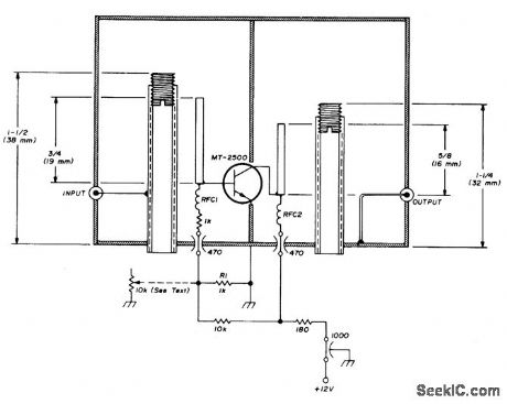
Narrow-band stage using Fairchlld MT-2500 bipolar transistor gives gain of 6 to 9 dB and noise figure of 2.5 to 4.5 dB.Cavity resonators at both input and output give excellent frequency selectivity. Similar circuit can be used wi1h Fairchild MT-4500, FMT-4005, or equivalent newer stripline-type transistors.RFC1 is 3 turns and RFC2 is 5 turns, air-wound with No. 26 enamel by using No. 52 drill as mandrel. Coupling strips on base and collector of transistor are 0.25-mm brass shim stock. Article gives construction and tune-up details, along with altemate design for HP-35821E and HP-35862E transistors using coupling loops. 10K pot is used only during tune-up.-N. J. Foot, Nanow-Band Solid-State 2304-MHz Preampli-fiers, Ham Radio, July 1974, p 6-11.
(View)
View full Circuit Diagram | Comments | Reading(631)
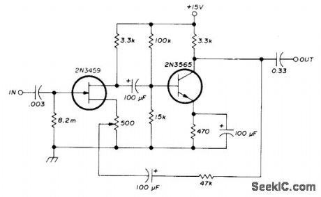
SMALL_SIGNAL_AMPLlFlER
Published:2009/6/24 23:31:00 Author:May

Combines fea-tures of virtual-earth and high-inpufimpedan ce amplifiers economically for such applications as a record amplifier, and provides several times the gain of a virtual-earth amplifier alone.-D.Rawson-Harris, Small Signal Amplifier, Wire-less World, Feb. 1977, p 45. (View)
View full Circuit Diagram | Comments | Reading(616)
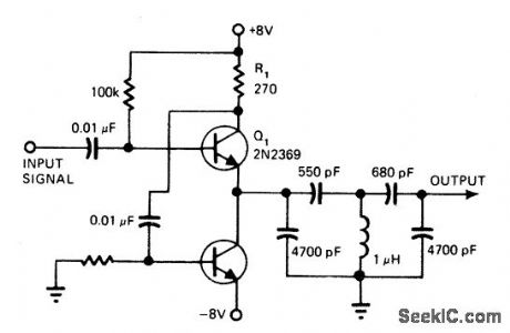
BASIC_FEEDBACK_AMPLlFlER
Published:2009/6/24 23:30:00 Author:May
Combination of unipolar and bipolar transistors gives desirable amplifying features of each solid.state device.Circuit can be optimized for RF or AF by ad justing coupling, feedback, and emitter bypass capacitor values. Changes in feedback affect dis-tortion, frequency response, and gain stability.To optimize for RF reduce capadtor sizes. For both AF and RF response, capacitors shown can be paralleled by small ceramic or Mylar units. If FET and bipolar are selected for high transcon-ductance and high gain-bandwidth product, overall voltage gain can be 20 or more for fre-quencies up to several megahertz.-I. M. Gott-Iieb,A New Look at Solid- State Amplifiers, Ham Radio, Feb. 1976, p 16-19. (View)
View full Circuit Diagram | Comments | Reading(774)
CAPACITIVE_LOAD_EMITTER_FOLLOWER
Published:2009/6/24 23:29:00 Author:May
Overcomes problem that develops with trailing edges of pulses when emitter-follower using NPN transistor is driving heavily capacitive load. Extra transistor is used to dump capacitor charge when emitter-follower stops conducting at trailing edge of input waveform. Pulse trailing edge thus tends to cut off a, and saturate lower transistor so it discharges capacitor. Circuit works equally well with pulses, square waves,and sine waves Transistors need not bematched Reverse polarity of supplies to usePNP transistors Useful for driving long coaxlines or logic from high-impedance source,without inversion,-H.L.Morgan,Emitter Follower's Fall Time Is Independent of Load、EDN Magazine Feb,5,1977,p 105 (View)
View full Circuit Diagram | Comments | Reading(1316)
23O_W_WATER_COOLED
Published:2009/6/24 23:35:00 Author:Jessie
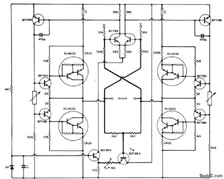
Used to excite mag-netic specimens in frequency range of 0 to 110 kHz at outputs up to 12 A. Output stage uses two complementary pairs of emitter-followers connected so each pair forms half of bridge, using MJ4030 and MJ4033 Darlingtons mounted on Iiquid-cooled heatsinks. Article describes cooling arrangement and circuit opera-tion in detail and gives suitable preamp circuit for driving inputs of BCY89 dual transistor. De-signed for 32-VDC supply, which connects to top and bottom horizontal buses on diagram.Feedback circuit are drawn in heavy lines. Re-sistors in series with Darlingtons (OR25, representing 0.25 ohm) are wound from resistance wire since they must carry large currents. Output impedance of circuit is less than 0.5 ohm, for matching to low-resistance load.-I. L. Ste-fani and II. Perryman, Liquid-Cooled Power Am-plifier, Wireless World, Dec. 1974, p 505-507. (View)
View full Circuit Diagram | Comments | Reading(670)
PARAPHASE_PHASE_INVERTER
Published:2009/6/24 23:34:00 Author:Jessie

Uses 180° phase difference between source and drain out-puts of Siliconix Ut83 FET to convert AF input to push-pull output without transformer. Volt-age gain in each half of circuit is about 0.8. Frequency response referred to 1 kHz is flat within 3 dB from 50 Hz to 50 kHz, when using lmeg-ohm output load.-R. P. Turner, FET Circuits, Howard VV. Sams, Indianapolis, IN, 1977, 2nd Ed.,p 29-30. (View)
View full Circuit Diagram | Comments | Reading(1908)
200_kHz_LINE_CARRIER_TRANSMITTER_WITH_ON_OFF_CARRIER_MODULATOR
Published:2009/6/24 23:16:00 Author:Jessie
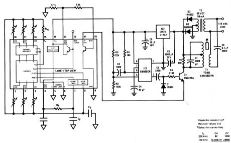
View full Circuit Diagram | Comments | Reading(2242)
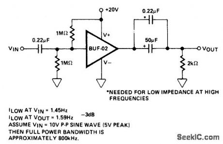
HIGH_SPEED_SINGLE_SUPPLY_AC_BUFFER
Published:2009/6/24 22:52:00 Author:May
View full Circuit Diagram | Comments | Reading(549)
10_×_BUFFER_AMPLIFIER
Published:2009/6/24 22:51:00 Author:May

View full Circuit Diagram | Comments | Reading(490)
SRABLE_HIGH_IMPEDANCE_BUFFER
Published:2009/6/24 22:50:00 Author:May

View full Circuit Diagram | Comments | Reading(446)
CMOS_BIPOLAR_VOLTAGE_FOLLOWER
Published:2009/6/24 23:12:00 Author:Jessie
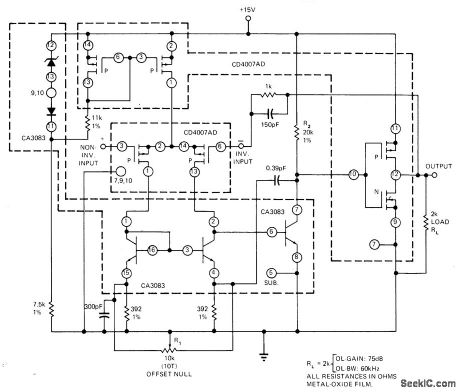
Combination of two 4007 CMOS gate packages andone CA3083 transistor package provides gain of about 75 dB as voltage-follower amplifier and bandwidth of 50 kHz. Slew rate is about 30V/μs, and settling time is 2 ps. Requires only single +15 V supply. Can be driven to within 1 mV of ground. Interfaces well with singlsupply D/A converters.-B. Furlow, CMOS Gates in Linear Applications: The Results Are Surpris-ingly Good, EDN Magazine, March 5, 1973, p 42-48. (View)
View full Circuit Diagram | Comments | Reading(944)
Indudes_general
Published:2009/6/24 23:11:00 Author:Jessie
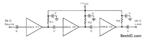
purpose RF amplifiers covering various portions of spectrum from DC to 2.3 GHz at outputs up to 230W, some with voltage-controlled gain, for pulses as well as video and other RF signals. See other chapters in book for RF amplifiers having specific applications.
0.25-400 MHz CASCADE-Three hybrid nlodules in cascade provide gain of 43.5 dB with flatness of ±1 dB over frequency range. Circuit draws 44 mA from 12-VDC supply. Modules 1 and 2 are Motorola MWA110, and module 3 is MWA120. All capacitors are 0.018μF. R1 and R2 are 1K,and R3 is 300 ohms,-“Wideband HybridAmplifiers、”Motorola,Phoenix,AZ, 1978、DS 5712 (View)
View full Circuit Diagram | Comments | Reading(678)
100_×_BUFFER_AMPLIFIER
Published:2009/6/24 22:49:00 Author:May
View full Circuit Diagram | Comments | Reading(476)
HIGH_RESOLUTION_ADC_INPUT_BUFFER
Published:2009/6/24 22:47:00 Author:May

View full Circuit Diagram | Comments | Reading(539)
| Pages:151/250 At 20141142143144145146147148149150151152153154155156157158159160Under 20 |
Circuit Categories
power supply circuit
Amplifier Circuit
Basic Circuit
LED and Light Circuit
Sensor Circuit
Signal Processing
Electrical Equipment Circuit
Control Circuit
Remote Control Circuit
A/D-D/A Converter Circuit
Audio Circuit
Measuring and Test Circuit
Communication Circuit
Computer-Related Circuit
555 Circuit
Automotive Circuit
Repairing Circuit