
Amplifier Circuit
Index 149
118_136_MHz_BROADBAND
Published:2009/6/25 21:24:00 Author:May

Designed for lowlevel amplitude modulation system. 50-ohm line transf ormers arewound with copperribbon on ferrite core to give 4:1 ratio. Design and con-struction procedures are covered. Transistor is Motorola 2N6083 rated 30 W for 4-W input.-B.Becciolini, Impedance Matching Networks Ap-plied to R-F Power Transistors, Motorola, Phoenix, AZ, 1974, AN-721, p 17. (View)
View full Circuit Diagram | Comments | Reading(1097)
100_W_FOR_DC_TO_500_kHz
Published:2009/6/25 21:32:00 Author:Jessie

Circuit using Optical Electronics opamps has high input imped-ance, high gain capability, and 100-W output capacity without use of transformers, for highfidelity audio circuits, cathode-ray deflection circuits, and servosystems. Output currents up to 10 A require heavy output wiring, large power-supply bypass capacity, and heavy com-mon ground point. Load is in feedback loop of opamp. Constant-current drive for load makes impedance matching to loudspeaker unnecessary.- A High Gain 100 Watt Amplifier, Optical Electronics, Tucson, AZ, Application Tip 10205. (View)
View full Circuit Diagram | Comments | Reading(777)
VOLTAGE_CONTROLLED_GAIN
Published:2009/6/25 21:32:00 Author:Jessie

2N5457 FET acts as voltage-variable resistor between differential inputterminals of opamp. Resistance vat-iation is linear with voltage over several decades of resistance, to give excellent electronic gain control. Values of resistors depend on opamp used.- FET Databook, National Semi-conductor. Santa Clara, CA, 1977, p 6-26-6-36. (View)
View full Circuit Diagram | Comments | Reading(5574)
HIGH_INPUT_IMPEDANCE
Published:2009/6/25 21:31:00 Author:Jessie

Simple JFET inputcircuit is operated as source follower with bootstrapped gate bias resistor and drain to give maximum possible reduction in input capacitance. Used as unity-gain AC amplifier.- FET Databook, National Semiconductor, Santa Clara, CA, 1977, p 6-26-6-36. (View)
View full Circuit Diagram | Comments | Reading(2)
10_dB_GAIN_AT_001_1OO_MHz
Published:2009/6/25 21:17:00 Author:May

High-gain wideband untuned general-purpose amplifier uses Fairchild 2N5126 or equivalent transistors in direct-coupled circuit. Design is stable for both power supply and temperature variations.Gain is adjusted with R1, with maximum of 38 to 44 dB and maximum output of about 1V P-P.Will drive low-level transistor circuits having load of about 1000 ohms. If several amplifiers are used in series for higher gain, shielding is required. Applications include amplification of pulsed light signals detected by photodiode. Cx can be 100-pF mica,-A. B Hutchison, Jr., Gen-eral Purpose Wide Band Amplifier, CQ, May 1972, p 22-23. (View)
View full Circuit Diagram | Comments | Reading(805)
HIGH_Z_PREAMP
Published:2009/6/25 21:16:00 Author:May

Provides up to 20 megohms of input impedance and has essentially flat response from 10 Hz to 220 MHz Q3 serves as emitter resistorfor Q2、and emitter-follower Q4 reduces loading Input impedance is further increased by adding optionalcomponents shownin dashed lines, Transistors are 2N2188,SK3005,GE-9、or HEP-2.-Circuits, 73 Magazlne,Feb,1974、p102. (View)
View full Circuit Diagram | Comments | Reading(829)
SHIFT_REGISTER_DRIVER
Published:2009/6/25 21:14:00 Author:May

A 16 V power supply can be synthesized as shown using IN1692 rectifiers. A shift pulse input saturates the 2N2714 depriving the Darlington combination (2N2714 and 2N2868) of base drive. The negative pulse so generated on the 15 V line is differentiated to produce a positive trigger pulse at its trailing edge. (View)
View full Circuit Diagram | Comments | Reading(0)
1_36_MHz_DISTRIBUTED
Published:2009/6/25 21:23:00 Author:Jessie

ProvkIes 18-dB gain over entire frequency range without use of special ferrite transformers, Gain contribution of each transistor, in phase with amplified wave as it passes down artificial transmission line, adds to that of other transistors. Capacitors marked with asterisks are lowinductance ceramic types such as Efie Redcap. Delay-line inductors L are 12 turns No.24 closewound on 1/8-inch diameter Lucite rod, and L/2 units are 7 turns. Can be used as preamp for frequency counter and as auxiliary for other test equipment. Article covers construction, heatsinking of transistor, and testing.-H. Olson, WidRange Broadband Amplifier, Ham Radio, April 1974, p 40-44. (View)
View full Circuit Diagram | Comments | Reading(1181)
BIAS_SUPPLY_FOR_CLASS_AB
Published:2009/6/25 21:23:00 Author:Jessie

Two-transistor supply using PNP silicon transistor as amplified diode variable-voltage source gives improved-performance transistor RF power amplifier op-erating in class AB Iinear mode. Transistor types are not critical, Output impedance of bias source is about 1 ohm, and output voltage changes only up to 3 1/2 for ±2.5 V change in input voltage Vcc.-C. P, Bartram, Bias Supply for R,F. Power Amplifiers, Wireless World, April 1976,p61. (View)
View full Circuit Diagram | Comments | Reading(655)
200_MHz_CASCODE
Published:2009/6/25 21:12:00 Author:May

JFETs give low cross modulation, large signal-handling ability, and AGC action controlledby biasing upper cascode JFET. Neutralization is not needed.- FET Databook, National Semiconductor, Santa Clara, CA, 1977, p 6-26-6-36. (View)
View full Circuit Diagram | Comments | Reading(647)
FET_BIPOLAR_SOURCE_FOLLOWER
Published:2009/6/25 21:12:00 Author:May

Used where source follower with high output-voltage swing and voltage gain close to unity is re-quired. Circuit has constant-current bias supply.Combination of unipolar and bipolar transistors gives desirable amplifying features of each solid-state device,-I. M. Gottlieb, A New Look at Solid-State Amplifiers, Ham Radio, Feb. 1976, p16-19. (View)
View full Circuit Diagram | Comments | Reading(953)
CASCODE
Published:2009/6/25 21:16:00 Author:Jessie

Combination of unipolar and bipolartransistors gives desirable amplifying fea-tures of each solid-state device. Ideal for use whh tuned circuits in audio, video, IF, and RF applications.-I. M. Gottlieb, A New Look at Solid-State Amplifiers, Ham fladio, Feb. 1976, p16-19. (View)
View full Circuit Diagram | Comments | Reading(1125)
UNITY_GAIN_VOLTAGE_FOLLOWER
Published:2009/6/25 21:16:00 Author:Jessie

Mea-sured galnis 0.0997 V/V with an error of ±0.1% over ±1.5V swihg Circuit has infinite inputimpedance and zero bias current,Addition of dashed components to simple voltage-follower design gives near-perfect performance.-C. Andren, The Ideal Voltage Follower, EEE Magazine, Jan. 1971, p 63-64. (View)
View full Circuit Diagram | Comments | Reading(681)
WIDEBAND_VARIABLE_GAIN
Published:2009/6/25 21:14:00 Author:Jessie

FET selves as ourPur gain-controlled device in feedback loop of Optical Electronics 9906 opamp. Resistive T network has SD201 MOS transistor as ground leg, with resistor values dlosen so transistor is electrically dose to summing junction, automatically limiting total signal voltage. Resulting arrangement of voltage-controlled feedback and compensation gives variable-gain amplifier whh good linearity and constant wideband width for all gain Ievels.- Wideband Variable Gain Amplifier, Optical Electronics, Tucson, AZ, Application Tip 10277. (View)
View full Circuit Diagram | Comments | Reading(1237)
VOICE_ACTIVATED_SWITCH_AND_AMPLIFIER
Published:2009/6/25 21:14:00 Author:Jessie

View full Circuit Diagram | Comments | Reading(0)
VIDEO_AMPLIFIER
Published:2009/6/25 21:13:00 Author:Jessie
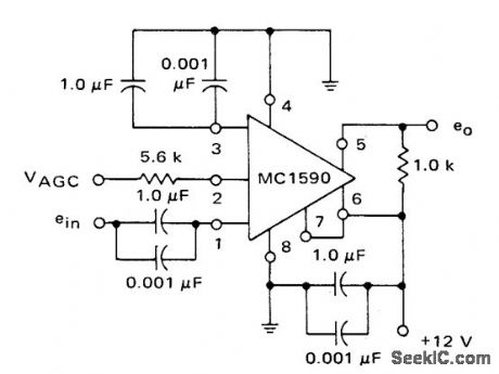
AGC capability of Motorola MC1590G makes h highly suitable for wideband video amplifier applications. Voltage gain is about 25 dB up to 50 MHz for 100-ohm load and 45 dB up to 10 MHz for 1K load. Several circuits can be cascaded to increase gain, using capacitive coupling.-B. Trout, A High Gain Inte-grated Circuit RF-IF Amplifier with Wide Range AGC, Motorola, Phoenix, AZ, 1975, AN-513, p9. (View)
View full Circuit Diagram | Comments | Reading(0)
HIGH_VOLTAGE_BUFFER
Published:2009/6/25 21:13:00 Author:Jessie
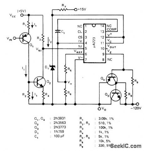


Circuit shown for μA723 voltage regulator permits use as highvoltage and high-current buffer in linear applications,Power dissipation of output transistor Q3 is only Iimiting factor,I1 is proportionalto VIN、I2 is proportional to I1, and output voltage Vo is proportional to I2 and VIN.-G. Niu, Single Op Amp Implements High-Voltage/Current Buffer, EDNMagazine, Oct 5, 1977, p 96 and 98 (View)
View full Circuit Diagram | Comments | Reading(1133)
VOLTAGE_CONTROLLED_AMPLIFIER_OR_TREMOLO_CIRCUIT
Published:2009/6/25 20:56:00 Author:May

The transistors form a differential pair with an active current-source tail. This config-uration, known technically as a variable-transconductance multiplier, has an output proportional to the product of the two input signals. Multiplication occurs due to the dependence o f the transistor transconductance on the emitter current bias. Tremolo (amplitude modulation of an audio frequency by a sub-audio oscillator-normally 5-15 Hz) applica-tions require feeding the low frequency oscil-lator signal into the optional input shown. The gain control pot maybe set for optimum depth. (View)
View full Circuit Diagram | Comments | Reading(971)
LINEAR_VARIABLE_DIFFFERENTIAL_TRANSFORMER(LVDT)DRIVER_DEMODULATOR
Published:2009/6/25 20:51:00 Author:May

View full Circuit Diagram | Comments | Reading(2537)
pH_PROBE_AMPLIFIER/TB_MPERATURE_COMPENSATOR
Published:2009/6/25 20:41:00 Author:May

View full Circuit Diagram | Comments | Reading(921)
| Pages:149/250 At 20141142143144145146147148149150151152153154155156157158159160Under 20 |
Circuit Categories
power supply circuit
Amplifier Circuit
Basic Circuit
LED and Light Circuit
Sensor Circuit
Signal Processing
Electrical Equipment Circuit
Control Circuit
Remote Control Circuit
A/D-D/A Converter Circuit
Audio Circuit
Measuring and Test Circuit
Communication Circuit
Computer-Related Circuit
555 Circuit
Automotive Circuit
Repairing Circuit