
Amplifier Circuit
Index 148
DIFFERENTIAL_CASCODE
Published:2009/6/25 22:43:00 Author:May

Direct-coupled single-stage amplifier with differential input and output can be used in one or more stages of high-performance ampimers. Bipolar-JFET caseode arrangement offers significant increase in common-mode input resistance and CMRR as compared to conventional diff erential pair, with little or no degradation of other performance parameters. Differential-mode gain is 116, commdnmode input resistanee is greater than 100 gigohms, CMRR is greaterthan 160 dB, and current-source output resistance is greater than 1 gigohm. Article gives design equations.-R. C.Jaeger and G. A. Hellwarth, Differential Cascode Amplifier Offers Unique Advantages, EDNMag-azine, June 5,1974, p 78 and 80. (View)
View full Circuit Diagram | Comments | Reading(920)
80_MHz_WITH_INPUT_PEAKlNG
Published:2009/6/25 22:41:00 Author:May

Response of CA3040 video IC is extended beyond 80 MHz in simple circuit that includes adjustable input peaking coil. Response is flatwithin 3 dBto well below t MHz, for gain of about 32 dB.-E. M Noll, Linear IC Principles, Experiments, and Projects, Howard W. Sams, Indianapolis, IN,1974, p163 and 169. (View)
View full Circuit Diagram | Comments | Reading(807)
WIDEBAND_BUFFER
Published:2009/6/25 22:31:00 Author:May

Low input capacitance of 2N5485 FET makes compound series-feedback buffer serve as wideband unity-gain amplifier having high input impedance.- FET Data-book, National Semiconductor, Santa Clara,CA,1977, p 6-26-6-36. (View)
View full Circuit Diagram | Comments | Reading(2334)
RAIN_ALARM
Published:2009/6/25 22:31:00 Author:May
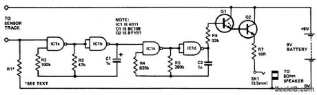
The circuit uses four NAND gates of a 4011 package. In eachoscillator, while one gate is configured as a straightforward inverter, the other has one input that can act as a control input. Oscillator action is inhibited if this input is held low. The first oscillator (IC1a and IC1b) has this input tied low via a high value resistor (R1) that acts as a sensitivity control. Thus this oscillator will be disabled until the control input is taken high. Any moisture bridging the sensor track will so enable the output which is a square wave at about 10 Hz. This in turn will gate on and off the 500 Hz oscillator formed by IC1c and IC1d. This latter oscillator drives the loudspeaker via R6, the Darlington pair formed by Q1 and Q2, and resistor R7. (View)
View full Circuit Diagram | Comments | Reading(3528)
CASCODE_RF_IF
Published:2009/6/25 22:31:00 Author:May

Uses half of SignetIcs 511 transistor array to provide voltage gain of about 10 over bandwidth of 2 MHz with output volt-age swing of 12V P-P. Design procedure is given. Circuit provides excellent isolation be-tween input and output.- Signetics Analog Data Manual, Signetics, Sunnyvale, CA,1971, p 746-747. (View)
View full Circuit Diagram | Comments | Reading(715)
168_MHz_BANDPASS
Published:2009/6/25 22:31:00 Author:May

Gain stage provides gain of 6 dB from 162 to 174 MHz. Skirt slope immediately outside passband decreases at 80 db/MHz. Uses dispersive-design surface-acous-tic-wave bandpass filter with 168-MHz center frequency, 7% bandwidth, and extremely steep skirt response. Parallel inductor at collector ter-minal matches capacitance of acoustic-wave device, and tapped inductor matches output terminal of filter to 50 ohms. Used in spread-spectrum communication receiver. Article cov-ers design and construction of filter on quartz substrate.-T.F.Cheek, Jr.,R.M.Hays,Jr.,and C.S.Hartmann, A Wide-Band Low-Shape-Fac-tor Amplifier Module Using an Acoustic Sur-face-Wave Bandpass Filter, IEEE Joumal of Solid-State Circuits, Feb. 1973, p 66-70. (View)
View full Circuit Diagram | Comments | Reading(691)
60_MHz_NARROW_BAND
Published:2009/6/25 22:30:00 Author:May

Signetics NE510/511 transistor array provides bandwidth of 0.5 MHz for 3dB down and noise figure of 7 dB for power gain of 30dB,Maximum output swing across 50 ohms is 300 mVRMS. Circuit is easily tuned.- Signetics Analog Data Manual. Signetics, Sunnyvale, CA,1977, p 749. (View)
View full Circuit Diagram | Comments | Reading(699)
SUMMING_AMPLIFIER
Published:2009/6/25 22:23:00 Author:May

Uses RCA CA3018 four-transistor array as current-mirror triad with low 4 mpedance buffered output, to serve as high-performance summing amplifier. Mea-sured harmonic distortion is less than 170 at voltage gains up to 50 and with output swing of 10V P-P. High output impedance of 51 kil-ohms can be buffered by Q2 connected as emitter-follower.-W.G.Jung. Monolithic-Triad Cument Summer, EDNIEEE Magazine, July 1,1971,p52. (View)
View full Circuit Diagram | Comments | Reading(1393)
RC_COUPLED_DIFFERENTIAL
Published:2009/6/25 22:10:00 Author:May

Input signal is applied to base of first differential amplifier and pushpull output is obtained from pins 8 and 10 for transfer to inputs of second IC. Feedback is transferred through RC combination back to pin 6 of first IC. Gain is varied with AGO voltage ap-plied to pin 2 of first IC. Gain is over 60 dB with flat response from 100 Hz to 100 kHz.-E.M.Noll, Linear IC Principles, Experiments, and Projects, Howard W. Sams, Indianapolis, IN, 1974, p 89-91. (View)
View full Circuit Diagram | Comments | Reading(769)
25_MHz_BANDWIDTH_LOW__NOISE
Published:2009/6/25 22:09:00 Author:May

RCA CA3018 fourtransistor array is connected as two pairs of common-emitter emitter-follower combinations, with two feedback loops providing high DC stabilhy. One path goes from emitter of Q3 back to input, and other goes from collector of Q4 to collector of Q1. Values of C1, C2, and C3 give low-frequency cutoff (3 dB down) of 800 Hz.Upper cutoff is 32 MHz.-E.M.Noll, Linear IC Principles, Experiments, and Projects, Howard W. Sams, Indianapolis, IN,1974, p 165-168 and 174. (View)
View full Circuit Diagram | Comments | Reading(776)
50_dB_BROADBAND_VIDEO
Published:2009/6/25 22:08:00 Author:May

RCA CA3018 fourtransistor array is connected as two pairs of common-emitter emitter-follower combinations, with two feedback loops providing high DC stabilhy. One path goes from emitter of Q3 back to input, and other goes from collector of Q4 to collector of Q1. Values of C1, C2, and C3 give low-frequency cutoff (3 dB down) of 800 Hz.Upper cutoff is 32 MHz.-E.M.Noll, Linear IC Principles, Experiments, and Projects, Howard W. Sams, Indianapolis, IN,1974, p 165-168 and 174.
(View)
View full Circuit Diagram | Comments | Reading(688)
RF_DIFFERENTIAL_AMPLIFIER
Published:2009/6/25 22:04:00 Author:May

Uses RCAC CA3028A linear IC to provide power gain ofabout 32 dB at frequencies up to about 120MHz,Values of tuned circuits deρend on frequency used Unmarked resistors are on IC -D.DeMaw、Vndelstanding Linear ICs、QST, Feb1977、p19 (View)
View full Circuit Diagram | Comments | Reading(745)
POLARITY_IGNORlNG_VOLTAGE_FOLLOWER
Published:2009/6/25 22:02:00 Author:May


Absolute-value circuit is basically voltage follower A1 whose input is positive regardless of polarity of VIN. With positive input, inverting amplifier A2 is disconnected by D1. With negative input, inverting amplifier applies poshive input to voltage follower through D1. Output voltage is thus absolute value of input voltage.-R. J. Wincentsen, Absolute Value Circuit Uses Only Five Parts, EDN Magazine, Nov. 1,1972, p 44. (View)
View full Circuit Diagram | Comments | Reading(1593)
VIDEO_ATTENUATOR
Published:2009/6/25 21:52:00 Author:Jessie

FETs in T attenuator provide optimum dynamic linear range for at-tenuation of video signals with ganged 1-meg-ohm pots. If complete turnoff is desired, atten-uatlon greater than 100 dB can be obtained at 10 MHz by using appropriate RF construction to minimize leakage. ON resistance of transistor (between drain and source) is less than 30 ohms.- FET Databook, National Semicon-ductor, Santa Clara, CA, 1977, p 6-26-6-36. (View)
View full Circuit Diagram | Comments | Reading(684)
PREAMP_F0R_O5_Hz_T0_2_MHz
Published:2009/6/25 21:50:00 Author:Jessie

Provides 11-dB gain over entire frequency range, with input impedance of 32 megohms. Q3 is GE-2 or HEP-52, and other transistors are SK3020 or HEP-53.-Circuits, 73Magazine, Jan. 1974, p 125. (View)
View full Circuit Diagram | Comments | Reading(749)
20_dB_VIDEO_LINE_DRIVER
Published:2009/6/25 21:50:00 Author:Jessie

RCA CA3100 wideband opamp and power transistor output stage together provide gain of 20 dB at video frequencies for driving 50-ohm line. Peak output voltage ranges from 8V at 1MHz to 1V at 8MHz Upper frequency limit for unity galn is about 38MHz.- Linear Integrated Circuits and MOS/FET's、″RCA Solid State Division,Somerville,NJ,1977,p 225-227 (View)
View full Circuit Diagram | Comments | Reading(1363)
50_MHz_POWER
Published:2009/6/25 21:49:00 Author:Jessie

Developed for use with 50 MHz microtransistor crystal oscillator,using additional GE microtransistor for boosting RF output to about 75 mW,Article covers construction with microcomponents and gives other microtransistor circuits for low-power amateur tadiouse and possible bugging applications,-B.Hoisington、Introduction to″Microtransistors,″73 Magazit, Oct.1974,p 24-30. (View)
View full Circuit Diagram | Comments | Reading(0)
CONSTANT_OUTPUT_IMPEDANCE
Published:2009/6/25 21:47:00 Author:Jessie

Pulse output stage gives output range from millivolts to 10 V P-P across 50 ohms while optimizing waveform characteristics of output pulse. With 2N2904 output transistors, circuit delivers 200 mA with 20-ms rise and fall times.-W. A. Palm, Pulse Amplifier Varies Amplitude, EDN Maga-zine, Aug. 5, 1978, p 76. (View)
View full Circuit Diagram | Comments | Reading(1067)
20_MHz_WIDEBAND
Published:2009/6/25 21:33:00 Author:May

RCA CA3040 IC is connected for single-ended input and balanced output, with no resonant circuits. Gain is above 30 dB over wide frequency range.-E. M. Noll, Linear IC Principles, Experiments, and Proiects, Howard W. Sams, Indianapolis, IN, 1974, p 162-163 and 168. (View)
View full Circuit Diagram | Comments | Reading(900)
DIFFERENTIAL_PAIR
Published:2009/6/25 21:25:00 Author:May

Conventional differential amplifier circuit provides differential-mode gain of 96, common-mode input resistance of 500 megohms, CMRR of 106 dB, and current-source output resistance greater than 1 gigohm. Article gives design equations.-R. C. Jaeger and G. A.Hellwarth, Differential Cascade Amplifier Offers Unique Advantages, EDN Magazine, June 5, 1974, p 78 and 80. (View)
View full Circuit Diagram | Comments | Reading(1002)
| Pages:148/250 At 20141142143144145146147148149150151152153154155156157158159160Under 20 |
Circuit Categories
power supply circuit
Amplifier Circuit
Basic Circuit
LED and Light Circuit
Sensor Circuit
Signal Processing
Electrical Equipment Circuit
Control Circuit
Remote Control Circuit
A/D-D/A Converter Circuit
Audio Circuit
Measuring and Test Circuit
Communication Circuit
Computer-Related Circuit
555 Circuit
Automotive Circuit
Repairing Circuit