
Circuit Diagram
Index 857
Light_target_flasher
Published:2009/7/19 23:27:00 Author:Jessie

Light target flasher. Photoresistor PC1 starts the flasher circuit whenever light hits it. Sensitivity control R1 is adjusted so that the flasher stops whenever the light source is removed (courtesy General Electric Company). (View)
View full Circuit Diagram | Comments | Reading(729)
LOW_NOISE_420_MHz_ATV_RECEIVER_CONVERTER
Published:2009/7/10 0:44:00 Author:May

L1, Q1, L2,and L3 compose an RF amp⒒fter stage that feeds Ml,a doubly balanced mixer. Q4 is alocal oscillator stage In the 375-MHz range.Signals h the 420ˉto 450-MHz range from Q1 are mixed in M1 and fed through filter L6/L7/C17,where only the 60- to 70-MHz (CH3/CH4) signals pass. The IF signal is passed to Q3, an IF amplifier. The overall gatrns 25 dB and the noise figure less than 2 dB. A kit of all parts,including the PC board,is available from North Country Radio, P.O. Box 53,Wykagyl Station,New Rochelle,NY 10804. (View)
View full Circuit Diagram | Comments | Reading(937)
INCREASED_FEEDBACK_STABILIZED_AMPLIFIER
Published:2009/7/10 0:41:00 Author:May
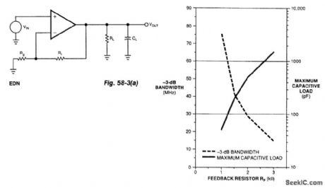
The usual method for using a current-feedback amplifier to drive a capacitive load isolates the load with a resistor in series with the amplifier's output.
A better solution involves only the amplifier's feedback resistors (Fig. 58-3(a)). Because the feedback resistors determine the amplifier's compensation, you can select the optimal value for these feedback resistors for almost any capacitive load.
Feedback resistance RF sets the amplifier's bandwidth. Increasing RF reduces the amplifier's band-width, which significantly improves the amplifier's ability to drive capacitive loads. Feedback resistor RG sets the amplifier's gain.
You cannot get the data necessary to calculate alternate values for RF from most data sheets. How-ever, a few minutes at the bench with a network analyzer will generate the data to make a graph of the value of the feedback resistor vs. the amount of capacitive load the amplifier can drive (Fig. 58-3(b)).
Start with the recommended data-sheet value for feedback resistor RF and measure the amplifier's frequency response without any capacitive load. Note the bandwidth, then add capacitive loading until the response peaks by about 5 dB. Record this value of capacitance; it is the maximum amount for that feed-back resistor. Then, increase the value of the feedback resistor and repeat the procedure until you develop a graph like the one in Fig. 58-3(b). (View)
View full Circuit Diagram | Comments | Reading(650)
13_watt_AF_power_amplifier_designed_for_an_8_ohm_or_4_ohm_load
Published:2009/7/20 1:49:00 Author:Jessie

13-watt AF power amplifier designed for an 8-ohm or 4-ohm load. The circuit needs only one power supply rated at 32 volts, 50 mA (courtesy GTE Sylvania Incorporated). (View)
View full Circuit Diagram | Comments | Reading(678)
DIGITAL_FREQUENCY_WINDOW
Published:2009/7/10 0:39:00 Author:May

This circuit detects frequency variation above or below preset limits. IC1 is a binary counter clocked at FCLK. The outputs are compared with switch preset values by IC2 and IC3. The input signal, which must be a positive-going pulse, is used to reset IC1. The P greater than Q output of the comparators is at logic 0 for input frequencies below the preset values. Above the preset count, a pulse train is output.IC2, detects a low input by supplying the pulse train to a retriggerable monostable, IC4. When the input frequency falls below the preset value in SW1, the monostable is no longer triggered and its output falls to logic 0. IC3 detects the frequency high state SW2, and outputs directly when this occurs. The outputs from both comparators can then be latched as shown, using IC5 and IC6. The clock frequency is related to input and switch values: switch value = FCLK/input. The time constant of IC4 is not critical, but must obviously exceed the maximum input pulse period. (View)
View full Circuit Diagram | Comments | Reading(845)
RADIO_BEACON_CONVERTER
Published:2009/7/10 0:39:00 Author:May

The radio beacon band extends from 280 to 516 kHz. Each beacon has its own characteristic AM-modulated morse-coded callsign that is transmitted on a specific frequency. To be able to receive distant beacons, the aerial signal is passed through a band-pass filter that effectively suppresses longwave and mediumwave signals. The ftlter also converts the aerial impedance, Zin, from about 10 kΩ to the input impedance of mixer IC1, which is about 1 kΩ.The mixer adds or subtracts the received signal to/from the local oscillator signal so that the beacon signal can be received on a normal shortwave receiver. The resulting frequencies are from 9.72 to 9.48 MHz or from 10.280 to 10.516 MHz. In the construction of the converter, some components must be surrounded by a metal shield, as indicated by dashed lines on the PC board layout.The circuit is aligned with the aid of an SSB receiver, to which the output of the convener is con-nected. Tune the receiver to 10 MHz and adjust the oscillator frequency of the converter with C8 for zero beat. Next, detune the receiver slightly until you hear a pleasant whistle, which is adjusted for minimum level with the aid of Pl. Finally, tune to a beacon transmitting at or about 300 kHz and adjust C13 for maximum sound output. (View)
View full Circuit Diagram | Comments | Reading(2130)
JFET_WIDEBAND_AMPLIFIER
Published:2009/7/10 0:37:00 Author:May

Using an MPF102 JFET, this circuit has a 50-Ω input impedance。Load impedance should be about 470Ω. A 3∶1 matching transformer can be used to get the impedance back to 50 Ω,This circuit will showabout 6- to 8-dB gam at VHF frequencies. (View)
View full Circuit Diagram | Comments | Reading(2256)
2_watt_AF_phono_amplifier_using_an_ECG740A_14_pin_DIP
Published:2009/7/20 1:48:00 Author:Jessie
2-watt AF phono amplifier using an ECG740A 14-pin DIP. Supply voltage is typically 18 volts. Voltage gain is 34 dB. Minimum audio power output is 2 watt, with 2.5 watts typical. When driving a 16-ohm load the supply voltage at pin 14 should be 24 volts (courtesy GTE Sylvania Incorporated). (View)
View full Circuit Diagram | Comments | Reading(739)
MOSFET_WIDEBAND_AMPLIFIER
Published:2009/7/10 0:35:00 Author:May
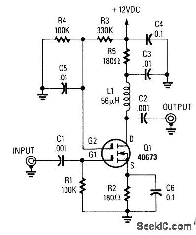
For high-impedance (7500 Ω) applications, this amplifter will provide a voltage gain of approximately -gm/ZL where ZL is the load impedance in ohms and gm is ≈ 12 x 10-3 for the 40673 FET. The G2 voltage can be used to control the gain. (View)
View full Circuit Diagram | Comments | Reading(1369)
LAMP_CONTROL_WITHOUT_CONDUIT
Published:2009/7/20 1:48:00 Author:Jessie

Motorola M0C3011 optoisolator permits control of large lamp,motor, pool pump, and other AC loads from remote location with low-voltage signal wiring while meeting building codes. Choice of triac depends on load being handled.-P.O'Neil, Applications of the MOC3011 Triac Driver, Motorola, Phoenix, AZ, 1978, AN-780, p 5. (View)
View full Circuit Diagram | Comments | Reading(1524)
HF_WIDEBAND_AMPLIFIER
Published:2009/7/10 0:34:00 Author:May

About 20-dB gain can be obtained using this IC. The gain can be controlled by varying the voltage applied to R3. (View)
View full Circuit Diagram | Comments | Reading(774)
ON_OFF_CONTROL_BY_THREE_TONES
Published:2009/7/20 1:46:00 Author:Jessie

Used for decoding two Touch-Tone digits to give operation or release of relay by remote control over wire line. Three 567 tone decoders and 7402 quad gate are adjusted to recognize tones corresponding to any two keys in given row or column on Touch-Tone keyboard. As example, * key generates 941 and 1209 Hz, and circuit can be adjusted so these two frequencies energize relay. Similarly, pushing of # key generates 941 and 1477 Hz that can be used for deenergizing relay.-W. J. Hosking, Simple New TT Decoder, 73 Magazine, April 1976, p 52-53. (View)
View full Circuit Diagram | Comments | Reading(1439)
500_MHz_AMPLIFIER
Published:2009/7/10 0:33:00 Author:May

This amplifier provides 1-W output at 500 MHz with a DV1202W FET. About 6- to 8-dB power gain can be expected. (View)
View full Circuit Diagram | Comments | Reading(738)
TWO_CA3100_WIDEBAND_OPERATIONAL_AMPLIFIERS
Published:2009/7/10 0:32:00 Author:May


These circuits use the RCA CA3100 wideband amplifier IC. The gain is:These circuits are useful for video applications to 10 MHz. The 3.3-pF capacitors are compensation capacitors. Capacitors on pins 7 and 4 are bypass capacitors to prevent self-oscillations. Figure 76-18(a) is noninverting and Fig. 76-18(b) is an inverting configuration. (View)
View full Circuit Diagram | Comments | Reading(664)
FACSIMILE_SWEEP_AMPLIFIER
Published:2009/7/20 1:46:00 Author:Jessie

Provides power amplification for driving electronic high-definition facsimile recorder. Sweep input voltage is high enough to eliminate need for voltage gain in power amplifier stages.-E. W. Van Winkl, High-Precision Sweep Generator, Electronics, 33:50. p 88-90. (View)
View full Circuit Diagram | Comments | Reading(582)
SIMPLE_TESLA_COIL
Published:2009/7/10 0:28:00 Author:May

The Tesla coil described here can generate 25,000 V. So, even though the output current is low, be very careful! The main component is a flyback transformer from a discarded TV.A new primary winding is needed. Begin by winding 5 turns of #18 wire on the core. Then, twist a loop in the wire, and finish 'ay winding five more turns. Wrap with electrical tape, but leave the loop exposed.A four-turn winding must be wound over the ten-turn winding that you've just finished. That is done the same way. First wind two turns of # 18 wire, then make a loop, and finish by winding two more turns.Again, wrap the new winding with electrical tape, leaving the loop exposed.When the windings are finished, the two loops shouldn't be more than 1/4-inch apart, but take care that they do not touch. Connect a 240-Ω resistor between the two loops. The modified transformer now should look like the one shown. Connect the transformer as shown. The 27-Ω resistor and two transistors should be mounted on a heatsH and must be insulated from it.The output of the high-voltage winding should begin to oscillate as soon as the circuit is connected to a 12-Vdc power supply. If it does not, reverse the connections to the base leads of the transistors. In normal operation, you should be able to draw 1-inch sparks from the high-voltage lead using an insulated screw-driver. (View)
View full Circuit Diagram | Comments | Reading(3715)
NINE_CHANNEL_CODER
Published:2009/7/20 1:45:00 Author:Jessie

Use of 'Ff L ICs gives low component count for remote control sys-tem having nine fully proportional channels. Input channels can be potentiometers for fully proportional information and switched resistors for go/no-go or multistep information.Coder scans the nine parallel inputs sequentially and presents them to single-line data link as series of nine varying-width pulses followed by fixed-width sync pulse. Article describes coder operation in detail and gives circuits for corresponding decoder and servoamplifier at receiving end of data link.-M. F. Bessant, Multi-Channel Proportional Remote Control, Wireless World, Oct. 1973, p 479-482. (View)
View full Circuit Diagram | Comments | Reading(795)
BALANCED_TMO_VCO
Published:2009/7/10 0:23:00 Author:May


This TMOS VCO operates in push-pull to produce 4 W at 70 MHz. It consists of two MFE930 TMOS devices in a balanced VCO that generally provide better linearity than the single-ended types. Varactors are not used because the design takes advantage of the large change in Miller capacitance, CRSS, that is available in TMOS gate structures.In the balanced VCO, the fundamental (fo) and/or twice the fundamental (2fo) can be coupled from the circuit at separate nodes. This makes the balanced oscillator very useful in phase-locked loops. The fundamental: (View)
View full Circuit Diagram | Comments | Reading(674)
Stereo_phono_AF_preamplifier_for_magnetic_pickups_using_the_ECG727
Published:2009/7/20 1:45:00 Author:Jessie

Stereo phono AF preamplifier for magnetic pickups using the ECG727. The schematic shows only one channel. Duplicate components must be used for channel B. Refer to the block diagram for pin identification. Voltage gain at t kHz is 47 dB. The ECG727 has four internal AC amplifiers (courtesy GTE Sylvania Incorporated). (View)
View full Circuit Diagram | Comments | Reading(649)
RAIL_FAULTDETECTING_AMPLIFIER
Published:2009/7/20 1:44:00 Author:Jessie

Signals from inductive pickup near rail are amplified enough to drive sensitive relay of pen recorder. Amplifier does not block after being overloaded when pickup passes over rail joint.-H. W. Keevil, Transistor Pulse Amplifiers Detect Rail Faults, Electronics, 35:21, p 53-54. (View)
View full Circuit Diagram | Comments | Reading(644)
| Pages:857/2234 At 20841842843844845846847848849850851852853854855856857858859860Under 20 |
Circuit Categories
power supply circuit
Amplifier Circuit
Basic Circuit
LED and Light Circuit
Sensor Circuit
Signal Processing
Electrical Equipment Circuit
Control Circuit
Remote Control Circuit
A/D-D/A Converter Circuit
Audio Circuit
Measuring and Test Circuit
Communication Circuit
Computer-Related Circuit
555 Circuit
Automotive Circuit
Repairing Circuit