
Circuit Diagram
Index 854
Continuous_indicator_using_an_LM3909_chip
Published:2009/7/19 23:53:00 Author:Jessie

Continuous indicator using an LM3909 chip. Circuitry inside dashes is the LM3909. The circuit actually flashes at a 2 kHz rate, which cannot be detected by the human eye. This indicator is not intended as a long life system since current drain is 12 mA (courtesy National Semiconductor Corporation). (View)
View full Circuit Diagram | Comments | Reading(496)
COMPOUND_OP_AMP
Published:2009/7/10 1:28:00 Author:May

By using an emitter-follower or a Darlington pair, a voltage-follower op amp configuration can source higher currents than the op amp otherwise could. (View)
View full Circuit Diagram | Comments | Reading(2356)
FLAT_TV_GENERATOR_MODULATOR
Published:2009/7/19 23:52:00 Author:Jessie

R-C gen erator V1, generating one of nine differ. ent carrier frequencies, feeds defection plate of beam deflection tube V2, while video modulation from camera is fed to grid 1 of V2 to modulate the carrier.-B. Binggeli and E. Fatuzzo, Solid-State Panels: Will They Bring Flat-Display TV?, Electronics, 35:26, p 67-70. (View)
View full Circuit Diagram | Comments | Reading(648)
WIEN_BRIDGE_OSCILLATOR
Published:2009/7/10 1:28:00 Author:May


This complex oscillator circuit uses a photocell and common-mode-suppression circuitry to achievedistortion of 0.0003%。 (View)
View full Circuit Diagram | Comments | Reading(0)
SIGNAL_DROPOUT_DETECTOR
Published:2009/7/10 1:28:00 Author:May

Used to Provide indiration of momentary dropout of d-c,a-c,or pulse input signal.lime between disappear of signal and indication of fault is adiustable. Outpul signal remains until scs is tumed off by momentarily opening reset switch.- Transistor Manual, Seventh Edition, Genercd Electric Co., 1964, p 336. (View)
View full Circuit Diagram | Comments | Reading(585)
6_volt_flasher_using_an_LM3909_chip
Published:2009/7/19 23:48:00 Author:Jessie


6-volt flasher using an LM3909 chip. Flashing rate is about 1 hertz. Circuitry inside dashed lines is the LM3909 (courtesy National Semiconductor Corporation).
(View)
View full Circuit Diagram | Comments | Reading(761)
RESISTANCE_TRIGG_FRED_ALARM
Published:2009/7/10 1:26:00 Author:May

Silicon controlled switch is triggered when temperature-, light-, or radication-sensifive resistor Rs up to meter drops below vadue of preset potentiometer.Interchanging Rs and potentiometer will trigger alarm on increase in sensing resistor.- Transi stor Manual, Seventh Edition, General Electric Co., 1964, p 425. (View)
View full Circuit Diagram | Comments | Reading(911)
THREE_DECADE_15_Hz_TO_15_kHz_WIEN_BRIDGE_OSCILLATOR
Published:2009/7/10 1:26:00 Author:May

In this circuit, an LM741 op amp drives a Wien-bridge network using two zener diodes as an ampli-tude limiter. Range selection is done 'oy switch selecting the capacitors (C1 through C6) and tuning is done via a ganged pot. The output is about 8 Vpp max., depending on the setting of S2 and R6. R4 is set for maximum distortion consistent with stable output. (View)
View full Circuit Diagram | Comments | Reading(1578)
SIGNAL_POWERED_ALARM_RECEIVER
Published:2009/7/10 1:25:00 Author:May

On arrival of carrier signal at frequency to which antenna and input are tuned, transistor pulls in relay applying battery power to horn or light. No power is drawn front battery during standby time. For signals below 50 Mc,best pick up is obtained with single-wire an tenna 150 feet long, at right angles to line.of-sight path and as high as possible.-L.R.Crump, Radio Waves Power Transistor Circulls, Electron'Ics, 31:19, p 63-65. (View)
View full Circuit Diagram | Comments | Reading(971)
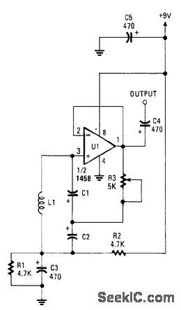
LOW_FREQUENCY_LO_OSCILLATOR
Published:2009/7/10 1:25:00 Author:May


Basically a Hartley oscillator using a triple-emitter follower, this oscillator can be used at audio and low radio frequencies. The frequency is given by:At 1 kHz, typically C would be 4.7 μF tantalums, but this is only a guide as to convenient values to use. (View)
View full Circuit Diagram | Comments | Reading(849)
Safe_high_voltage_flasher_using_an_LM3909
Published:2009/7/19 23:47:00 Author:Jessie
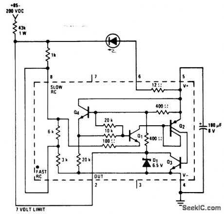
Safe high-voltage flasher using an LM3909. Circuitry inside dashes is the LM3909. If the 43K dropping resistor shown is employed the IC and LED will be about 7 volts above ground (courtesy National Semiconductor Corporation). (View)
View full Circuit Diagram | Comments | Reading(640)
VERY_LOW_DISTORTION_OSCILLATOR
Published:2009/7/10 1:24:00 Author:May

his oscillator uses a bridge circuit with an optoisolator as a gain-control device. The resultant distor-tion can be held to 9 ppm (.0009%) with proper adjustment. (View)
View full Circuit Diagram | Comments | Reading(693)
SIX_TRANSISITOR_9_V_BROASCAST_WITH_TUNED_R_F_STAGE
Published:2009/7/19 23:46:00 Author:Jessie

Nominal sensitivity is 30 microvolts per meter, power output 500 mw, and battery drain 12.5 ma.-“Transistor Manual,” Seventh Edition, General Electric Co., 1964, p 296. (View)
View full Circuit Diagram | Comments | Reading(617)
The function features of TOPSwitch—Ⅱ
Published:2011/7/20 23:27:00 Author:Borg | Keyword: function features, TOPSwitch—Ⅱ

The features of the TOPSwitch—Ⅱproducts:(1) all the functions of PWM control system are combined on the 3-terminal chip, which contains the PWM, power switch MOSFET, auto bias circuit, protection circuit, high voltage starting circuit and circuit compensation circuit, the output terminal and the grid are fully separated by the HF transformer, so the single chip integration of the auto frequency transformer, separator and reversed motivation switch power is completed, which is safe and reliable. (View)
View full Circuit Diagram | Comments | Reading(487)
PROGRAMMABLE_INVERTER_RECTIFER
Published:2009/7/10 1:23:00 Author:May


The op amp is alternately an inverter or buffer, under control of the switch polarity. As a buffer, the gain is always 1, but as an inverter, the gain is set by the ratio of the input and feedback resistors. By adding a comparator, the function can be synchronously switched as the input polarity changes, which ffectively rectifies the output. The output polarity is determined by the switch logic (normally open or normally closed) and the comparator input polarity. (View)
View full Circuit Diagram | Comments | Reading(681)
HIGH_STABILITY_3_35_MC_OSCILLATOR
Published:2009/7/19 23:43:00 Author:Jessie

Modification of Lampkin circuit uses pair of cathode followers in cascade, with tube circuits being tapped across part of coil and excited from resonator through high impedance. Bifilar choke minimizes variations in heater-cathode capacitance of driver V2.-E. Robberson, R-F Oscillator has Improved Stability, Electronics, 36:32, p 62-63. (View)
View full Circuit Diagram | Comments | Reading(993)
WIEN_BRIDGE_BASED_OSCILLATOR_WITH_VERY_LOW_DISTORTION
Published:2009/7/10 1:20:00 Author:May

This complex oscillator circuit uses a photocell and common-mode-suppression circuitry to achieve distortion of 0.0003%. This oscillator circuit replaces the lamp in the traditional Wien bridge with an elec-tronic equivalent. (View)
View full Circuit Diagram | Comments | Reading(880)
I_F_A_F_REFLEX
Published:2009/7/19 23:41:00 Author:Jessie

Single transistor gives simultaneous amplification at intermediate and audio frequencies in economy radio. Careful design provides high gain and sufficient un distorted output power to drive audio output transistor at full rating without motorboating.-J. Waring, How To Design Reflexed Transistor Receivers, Electronics, 32:19, p 70-72. (View)
View full Circuit Diagram | Comments | Reading(718)
500_MC_COLPITTS
Published:2009/7/19 23:41:00 Author:Jessie

Frequency varies less than 3 Mc from 25 to 75℃, and less than 1.5 Mc with bias change from 6 to 9 V. Output is 10 mw. T1 is 1.5 length of 3/8 brass rod with output tap 1/4 from bottom.-Texas Instruments Inc., Solid-State Communications, McGraw-Hill, N.Y., 1966, p 301. (View)
View full Circuit Diagram | Comments | Reading(675)
3_INPUT_AND_GATE_COMPARATOR
Published:2009/7/10 1:18:00 Author:May
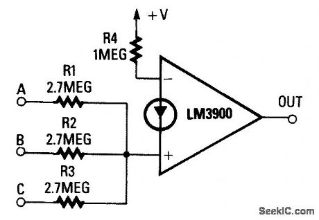
This circuit has high output onty when all three inputs are high. The noninverting-input current, when all three inputs are high, must exceed that of the inverting input, as determined by R4. The circuit can be converted to a NAND gate by transposing the two inputs of the op amp. (View)
View full Circuit Diagram | Comments | Reading(807)
| Pages:854/2234 At 20841842843844845846847848849850851852853854855856857858859860Under 20 |
Circuit Categories
power supply circuit
Amplifier Circuit
Basic Circuit
LED and Light Circuit
Sensor Circuit
Signal Processing
Electrical Equipment Circuit
Control Circuit
Remote Control Circuit
A/D-D/A Converter Circuit
Audio Circuit
Measuring and Test Circuit
Communication Circuit
Computer-Related Circuit
555 Circuit
Automotive Circuit
Repairing Circuit