
Circuit Diagram
Index 1059
555 Voltage-controlled Oscillator Circuit with its Duty Cycle Controlled by Vc Terminal
Published:2011/8/1 23:41:00 Author:Zoey | Keyword: 555 Voltage-controlled Oscillator Circuit, duty cycle , Vc terminal
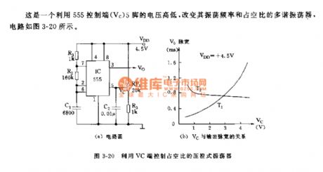

Circuit of the multi-vibratorhas beenshown in thepicture 3-20, oscillator frequency and duty cycle of the vibratorare adjusted according to the level on pin 5, which is controlled by 555 controlling terminal Vc.
A 555, R1, R2 and C1 together constitute an astable multi-vibrator. The controlling terminal can change the level it controlledthrough RP1,it also controls the voltage of comparator A1’s reverse terminal in the chip, adjusts comparator’s baseline voltage so as to change the turnover level of RS trigger and time constant of charge and discharge loop.
As illustrated in picture(b), we can take advantage of the oscillation pulse , which is voltage-controlled, to adjust the voltage of duty cycle without changing oscillation frequency, or to transfer the pulse width, pulse position as well as the voltage. Concrete operation can be seen in 5-26, 5-27 and 5-31,etc in chapter 5.
(View)
View full Circuit Diagram | Comments | Reading(1526)
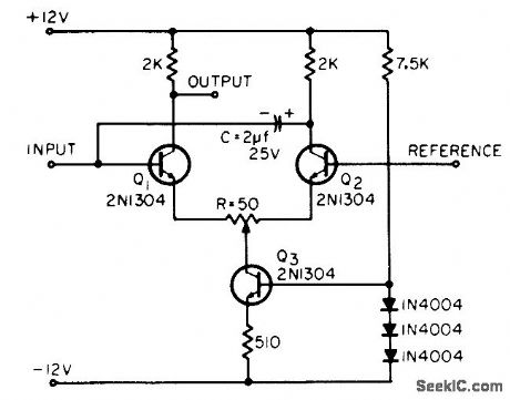
Basic_positive_reference__DAC
Published:2009/7/23 21:27:00 Author:Jessie
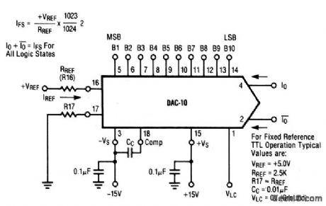
This circuit shows a DAC that is connected for positive-reference D/A-converter operation.
(View)
View full Circuit Diagram | Comments | Reading(467)
Microprocessor_supervisory_circuit
Published:2009/7/23 21:27:00 Author:Jessie
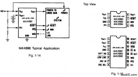
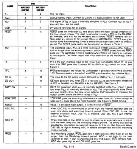
Figures 1-14 and 1-15 show a typical application circuit and block diagram, respectively, for the MAX690. The IC is similar to that described for Fig. 1-M, but also includes watchdog and battery-backup protection, and has a 1.3-V threshold detector, as shown in Fig. 1-16. Use the equations shown in Fig. 1-M to calculate the values for the resistors at the PFI input (except use a threshold of 1.3 V, instead of 2.54 V). MAXIM NEW RELEASES DATA Book, 1992, P. 5-19, 5-22. (View)
View full Circuit Diagram | Comments | Reading(1215)
LOW_HYSTERESIS_TRIGGER
Published:2009/7/23 21:26:00 Author:Jessie
Differential-amplifier pair, with constant-current source Q3 replacing emitter resistor, serves as level detector with low hysteresis. Good up to 60 kc.-D. B. Campbell, Low-Hysteresis Trigger Circuits, EEE, 13:1, p 76. (View)
View full Circuit Diagram | Comments | Reading(769)
Low_phase_shift_IF_limiter
Published:2009/7/23 21:26:00 Author:Jessie
The SL532 shown here is used for wide-bandwidth limiting IF strips.With the values shown, the input signal for full limiting is 300 μV (rms)(-57 dBm), the output is limited to 1 Vpp, with a phase shift of ±3%. (View)
View full Circuit Diagram | Comments | Reading(602)
Battery_manager
Published:2009/7/23 21:25:00 Author:Jessie
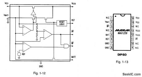
Figures 1-12 and 1-13 show the block diagram and pin configuration; respectively, for the MAX1259. The IC is similar to that described for Fig. 1-N, and switches to the backup battery when the primary power supply is interrupted. The input-output differential is 200 mV when supplying 250mA from the primary power or 15mA from the battery. The battery-failure output at pin 3 indicates when the battery is below +2 V. The power-fail output at pin 11 indicates when the primary power is low. MAXIM NEW RELEASES DATA BOOK, 1992, P. 5-17. (View)
View full Circuit Diagram | Comments | Reading(631)
PROTECTIVE_DIODES_FOR_SCHMITT_TRIGGER
Published:2009/7/23 21:25:00 Author:Jessie
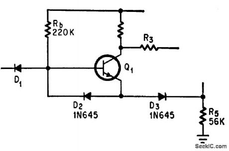
Addition of diodes D2 and D3 to modified Schmitt trigger having isolating diode D1 prevents reverse breakdown of emittor-base junction of Q1.-J. Gaon, Diode and Resistor Increase Input Resistance of Schmitt, Electronics, 39:12, p 110-111. (View)
View full Circuit Diagram | Comments | Reading(606)
AUTOMOBILE_IGNITION_SUBSTITUTE
Published:2009/7/6 2:14:00 Author:May
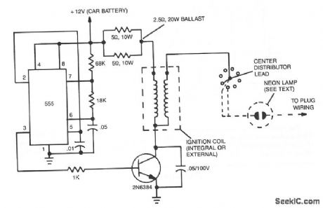
The ignition substitute provides a constant power source for the ignition coil. Its frequency, 0.5- 1.0 kHz, is that used by an 8-cylinder engine with an idling speed of 650 RPM, and the unit provides a rapid spark at a 17% duty cycle, while staying within the power dissipation limits of the components.
The circuit consists of a 555 timer IC configured as an astable free-running multivibrator that is used to drive a high-current npn transistor, such as a 2N6384. The transistor should be heavily heatsinked because it might be drawing several amps over quite a long period of time.
The coil ballast can be from 0.68 to 6.5Ω, depending on what's available. The 2.5-Ω, 20-W ballast shown works well. All the other resistors can be either 1/4- or 1/2-W devices, and the capacitor, between pins 1 and 5 of the 555, can range from 0.01 to 0.05 μF. Do not omit the 100-V, 0.05-μF capacitor across the transistor; it prevents voltage spikes from damaging the device.
Although designed for an 8-cylinder engine, this device can be used with other types. In addition,a neon bulb can be added to the circuit to verify the presence of a spark.
(View)
View full Circuit Diagram | Comments | Reading(722)
True_logarithmic_IF_amplifier
Published:2009/7/23 21:25:00 Author:Jessie
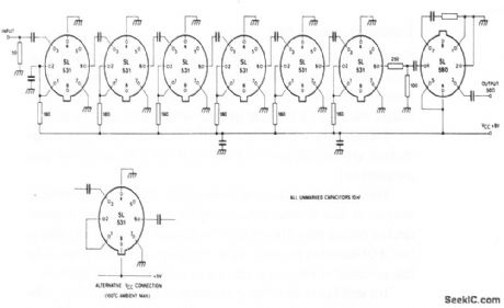
The SL531 shown here is a wide-band amplifier for use in IF circuits or strips ofthe true log type(where input and output are at the same frequency and nodetection Occurs) With the values shown,the frequency range is 10 to 200 MHz.An SL560 is used as a unity-gain buffer, the output of the log strip being attenuated before the SL560 to give a nominal 0-dBm output into 50Ω. The low-level gain is 60 dB with an output dynamic range of 20 dB. (View)
View full Circuit Diagram | Comments | Reading(649)
RECEIVER_MONITOR
Published:2009/7/6 2:13:00 Author:May

Circuit Notes
The alarm plugs into the earphone jack on a receiver. Then when a signal (normally fed to the headphones) is detected and applied to the gate of SCR1, it conducts, sounding whatever alarm is connected to SO1. The signaling device can be an audible alarm or a lamp. Variable resistor R1 functions as a sensitivity control so that background noises won't trigger the alarm. (View)
View full Circuit Diagram | Comments | Reading(722)
Microprocessor_monitor
Published:2009/7/23 21:25:00 Author:Jessie
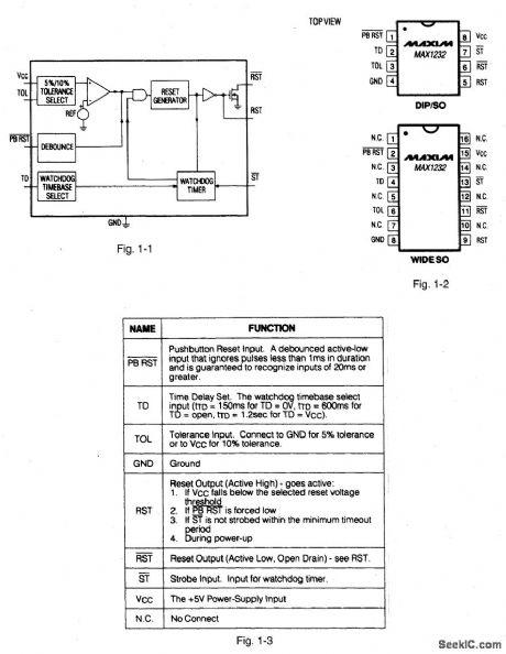
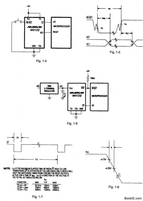
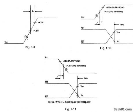
Figures 1-1, 1-2, and 1-3 show the block diagram, pin configuration and pin description, respectively, for the MAX1232. The IC is similar to that described for Figs. 1-K and 1-L, except that only '/to power is consumed. Figures 1-4 and 1-5 show the basic connections and waveforms, respectively, for the pushbutton reset.Figures 1-6 and 1-7 show the basic connections and waveforms, respectively, for watchdog timing. Notice that the software routine that strobes ST is critical. The code must be in a section of software that executes frequently enough so that the time between toggles is less than the watchdog timeout period, as shown in Fig. 1-7. Figures 1-8 and 1-9 show the power-down and power-up slew rate, respectively.Figures 1-10 and 1-11 show the VCC-detect reset-output delays. MAXIM NEW RELEASES DATA BOOK, 1992, P. 5-11, 5-14, 5-:5, 5-16. (View)
View full Circuit Diagram | Comments | Reading(669)
LOW_DRIFT_PEAK_DETECTOR
Published:2009/7/6 2:13:00 Author:May

This circuit uses op amp U1 to compensate for the offset in peak detector diode D1. Across Ch is the exact peak voltage; U2 is used as a voltage follower to read this voltage. (View)
View full Circuit Diagram | Comments | Reading(0)
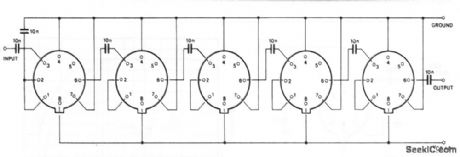
PNPN_SHIFT_REGISTER
Published:2009/7/23 21:24:00 Author:Jessie
Consists of five one bit memory elements connected in cascade.-J. B. Hangstefer and L. H. Dixon, Jr., Triggered Bistable Semiconductor Circuits, Electronics, 32:35, p 58-60. (View)
View full Circuit Diagram | Comments | Reading(538)
Audio_mixer_or_selector
Published:2009/7/23 21:22:00 Author:Jessie

This circuit uses the four Norton amplifiers of an LM3900 to form an audio-mixing or selection circuit (Norton amplifier circuits are also shown in chapter 11). With this circuit,particular amplifiers can be gated off with dc-control signals applied to the (+) inputs. Amplifier 3 is active, with SW3 closed, while amplifiers 1 and 2 are driven into saturation by the +V input applied through the 5.1 -M resistors. (View)
View full Circuit Diagram | Comments | Reading(2180)
5_V_AT_5_A_WITH_IC_SWITCHER
Published:2009/7/6 2:12:00 Author:May

Uses Silicon General SG1524 IC as pulse-width-modulated regulator for which operating frequency remains constant, with ON time of each pulse adjusted to maintain desired output voltage. Operating range extends above 100 kHz but device draws only 10 mA. IC includes voltage reference, oscillator, comparator, error amplifier, current limher, pulse-steering flip-flop, and automatic shutdown for overload.-P. Franson, Today's Monolithic Switching Circuits Greatly Simplify Power-Supply Designs, EDN Maga-zine, March 20, 1977, p 47-48, 51, and 53. (View)
View full Circuit Diagram | Comments | Reading(1950)
5_30_V_AT_15_A
Published:2009/7/6 2:11:00 Author:May
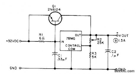
External series-pass transistor boosts 500-mA rated output of 78MG or 79MG regulator to 1.5 A for use as adiustable power supply in lab. Circuit has no short-circuit protection for safe-area limiting for external pass transistor, but article shows how to add protective transistor for this purpose.-J. Tru-Iove, A New Breed of Voltage Regulators, 73 Magazine, March 1977, p 62-64. (View)
View full Circuit Diagram | Comments | Reading(1708)
_50_V_FLOATING
Published:2009/7/6 2:10:00 Author:May

RCA CA723 regulator operating from 85-V supply delivers 50 V with Iine regulation of 15 mV for 20-V supply change and load regulation of 20 mV for 50-mA load current change.- Linear Integrated Circuits and M0S/ FET' s, RCA Solid State Division, Somerville, NJ, 1977, p 61. (View)
View full Circuit Diagram | Comments | Reading(874)
TYPICAL_SCHMITT_TRIGGER
Published:2009/7/23 21:21:00 Author:Jessie
Performs well at frequencies up to 100 kc. Capacitor may be removed for low-frequency operation. Widely used to produce square wave from sinusoidal input, because regenerative circuit changes states abruptly when input signal crosses specific d-c triggering levels.-Texas Instruments Inc., Transistor Circuit Design, McGraw-Hill, N.Y., 1963, p 382. (View)
View full Circuit Diagram | Comments | Reading(825)
SIMPLIFIED_UJT_SCR_TRIGGER
Published:2009/7/23 21:30:00 Author:Jessie
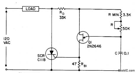
Emitter timing circuit and base-2 of ujt are supplied directly from ac line, with dropping resistor RD keeping peak voltage on ujt within specifications.- Transistor Manual, Seventh Edition, General Electric Co., 1964, p 329. (View)
View full Circuit Diagram | Comments | Reading(1989)
High_performance_supervisory_circuit
Published:2009/7/23 21:30:00 Author:Jessie
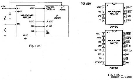
Figures 1-24 and 1-25 show a typical application circuit and pin configurations, respectively, for the MAX790/791. The IC is similar to the MAX690 series (Figs. 1-14 and 1-15), but with several improvements, including 70-μA supply current, 10-ns CE propagation delay, 250-mA output current (VCC mode), and 25-mA output current (VBATT mode). The MAX790 is pin compatible with the MAX690. The reset output is guaranteed to be in the correct state for VCC down to 1 V. MAXIM NEW RELEASES DATA BOOK, 1992, P. 5-53. (View)
View full Circuit Diagram | Comments | Reading(565)
| Pages:1059/2234 At 2010411042104310441045104610471048104910501051105210531054105510561057105810591060Under 20 |
Circuit Categories
power supply circuit
Amplifier Circuit
Basic Circuit
LED and Light Circuit
Sensor Circuit
Signal Processing
Electrical Equipment Circuit
Control Circuit
Remote Control Circuit
A/D-D/A Converter Circuit
Audio Circuit
Measuring and Test Circuit
Communication Circuit
Computer-Related Circuit
555 Circuit
Automotive Circuit
Repairing Circuit