
Index 157
PULSE_WIDENER
Published:2009/7/15 5:19:00 Author:Jessie
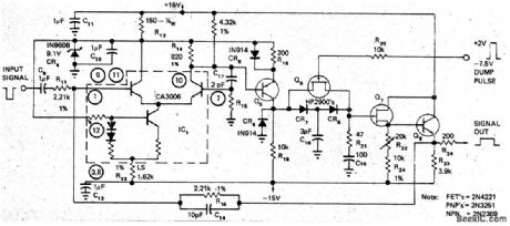
Peak detection diodes CR7 and CR8 in feedback loop of unity-gain CA3006 differential opamp form peak holder that maintains amplitude of narrow video pulses while stretching output pulses as much as 6000 times (from 50 ns to as much as 300 μs). Gain of circuit is unity. Article describes timing and control circuits required in conjunction with peak holder to achieve predictable termination times for stretched pulses, These external circuits include μA710 used as threshold limiter, 9602 dual monostable used as delay-pulse and dump-pulse timing generators, and discrete transistor stage serving as dump-pulse output stage.-B. Pearl, Peak Holder Stretches Narrow Video Pulses, EDN Magazine, Feb. 5, 1973, p 46-47 (View)
View full Circuit Diagram | Comments | Reading(874)
VARIABLE_ON_TIME
Published:2009/7/14 2:57:00 Author:May
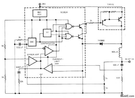
Duty cycle of SG3524 switching regulator is varied by modulating ON time while maintaining constant switching frequency, using pulse- du ration-modulation control circuit.-J. Spencer, Monolithic Switching Regulators-They Fit Today's Power-Supply Needs, EDN Magazine, Sept. 5, 1977, p 117-121.
(View)
View full Circuit Diagram | Comments | Reading(649)
THREE_DIODES_PROVIDE_8_STATES
Published:2009/7/14 2:57:00 Author:May
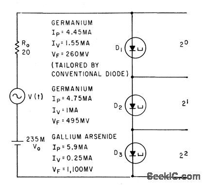
Three different tunnel diodes, each switching at a different input voltage level, act together to convert analog input voltage to digital form.-B. Rabinovici and J. Klapper, Designing Tunnel-Diode Circuits Using Composite Char-acteristics, Electronics, 35:7,p 46-48. (View)
View full Circuit Diagram | Comments | Reading(505)
16_FUNCTIONS_OF_X_AND_Υ
Published:2009/7/14 2:56:00 Author:May
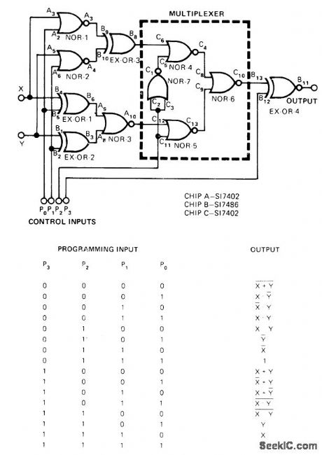
With only three IC chips, circuit provides choice of any one of 16 possible functions of two Boolean variables, Table shows output states for all programming combinations of control inputs P.-S. Murugesan, Programmable Logic Circuit Has Versatile Outputs, EDN Magazine, Feb. 5, 1975,p 57. (View)
View full Circuit Diagram | Comments | Reading(572)
TRANSFORMERLESS_SCR_BRIDGE_INVERTER
Published:2009/7/15 5:17:00 Author:Jessie

Slave-triggering of SCR1 and SCR2 with capacitive load cuts cost in half by eliminating costly gate transformers. Input of 800 pps (both half-cycles of 400-cps mvbr) gives 400-cps sine. wave output with peak amplitude of 350 v, because bridge switching inverts alternate pulses.-L. M. Tibbets, Scr Bridge Inverter Eliminates Transformers, Electronics, 39:18, p 98-99. (View)
View full Circuit Diagram | Comments | Reading(1766)
5_V_AT_1_A
Published:2009/7/14 2:55:00 Author:May

National LM122 timer is connected as switching regulator by using internal reference and comparator to drive switching transistor Q1. Minimum input voltage is 5.5 V. Line and load regulation are less than 0.5%, and out-put ripple at switching frequency is only 30 mV. Output voltage can be adjusted between 1 V and 30 V by using appropriate values for R2-R5.-C. Nelson, Versatile Timer Operates from Microseconds to Hours, National Semiconductor, Santa Clara, CA, 1973, AN-97, p 9. (View)
View full Circuit Diagram | Comments | Reading(1357)
VARIABLE_TRANSCONDUCTANCE_DIVIDER
Published:2009/7/14 2:55:00 Author:May
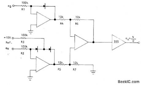
Practical analog divider follows ideal division equation over typical 20:1 range of reference current and operates in two quadrants. Circuit is analyzed in terms of logarithmic behavior of its elements. Bandwidths up to 5 MHz can be achieved. Article gives design equations.-L.Counts and D. Sheingold, Analog Dividers: What Choice Do You Have?, EDN Magazine, May 5, 1974, p 55-61. (View)
View full Circuit Diagram | Comments | Reading(783)
10_W_FOR_220_MHz
Published:2009/7/14 2:54:00 Author:May
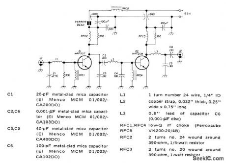
Class C RF power amplifier for VHF FM transmitter has stable gain of 20 dB for operating bandwidth of 40 MHz. Article gives design procedure using Smith chart and covers construction and tune-up.-J. DuBois, 220-MHz BF Power Amplifier for VHF FM, Ham Radio, Sept. 1973, p 6-8. (View)
View full Circuit Diagram | Comments | Reading(2785)
SEQUENTIAL_PULSES
Published:2009/7/15 5:15:00 Author:Jessie
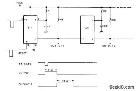
Any number of sections of 554 quad monostable timer can be cascaded as shown to give sequential series of output pulses of widths determined by values of R and C. No coupling capacitors are required because timer is edge-triggered. Negative reset pulse simultaneously resets all sections. Varying control voltage (in range of 4.5-16V) affects period of all timer sections simultaneously.-H.M. Berlin, IC Timer Review, 73 Magazine, Jan.1978, p 40-45. (View)
View full Circuit Diagram | Comments | Reading(531)
VIDEO_PROCESSOR
Published:2009/7/14 2:53:00 Author:May
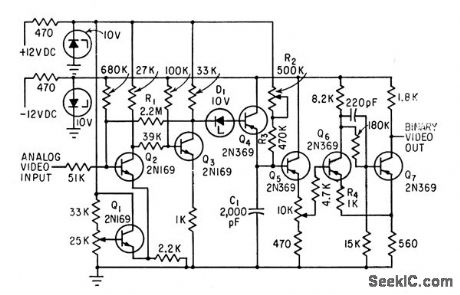
Analog video input from closed-circuit tv microscope is converted to binary video output by difference amplifier Q1-Q2, squaring amplifier Q3, pulse shaper Q4, and emitter-follower Q5 which buffers R-C network from Schmitt trigger Q6-Q7.-N. F. Izzo and W. Coles, Blood-Cell Scanner Identifies Rare Cells, Electronics, 35:17, p 52-57. (View)
View full Circuit Diagram | Comments | Reading(693)
PHONE_IN_USEINDICATOR
Published:2009/7/14 2:52:00 Author:May
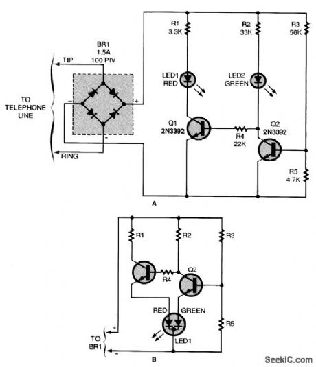
Tired of having your phone calls interrupted by others picking up the receiver? This circuit (A) will show others when the phone is in use. If you would like to experiment with a tricolor LED, check out the optional schematic (B).
When all telephones are on-hook, Q2's base is turned on by a voltage-divider circuit, consisting of R3 and R5. (The value shown for R5 causes the device to switch over at about 9 V; it can be changed to facilitate other voltage levels.) Transistor Q2 allows current to flow through R2 and LED2, indicating that the phone line is not in use. It also effectively grounds the base of Q1 and forces LED1 to remain off. When the voltage drops because a telephone goes off-hook, Q2 stops con-ducting, which allows a little current to flow from R2, LED2, and R4 to Q1's base. When that occurs, Q1 conducts, energizing LED1 and LED2 is deprived of sufficient current to glow. The bridge rectifier compensates for a possible reversal between the tip and ring wires, and rectifies the ring signal. (View)
View full Circuit Diagram | Comments | Reading(613)
UJT_CONVERTER_FOR_ACCELEROMETER
Published:2009/7/14 2:52:00 Author:May
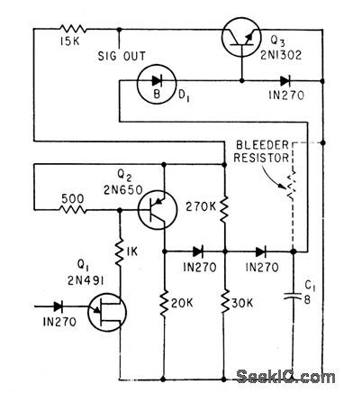
Converts digital output to voltage analog that indicates rate of acceleration or, when bleeder resistor is removed, actual distance traveled.-F. W. Kear, Unijunction Transistor Pulse-Circuit Design, Electronics, 35:21,p 58-60. (View)
View full Circuit Diagram | Comments | Reading(690)
UNITY_GAIN_INVERTER
Published:2009/7/15 5:10:00 Author:Jessie
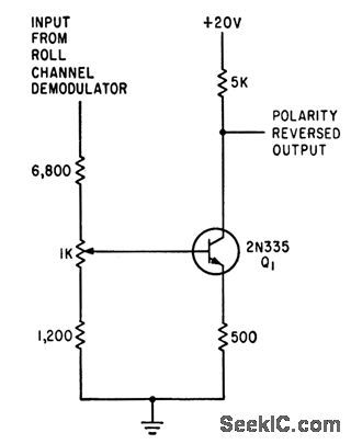
Provides for differential roll motion of missile autopilot.-J. H. Porter, Miniaturized Autopilot System for Missiles, Electronics, 33:43, p 60-64. (View)
View full Circuit Diagram | Comments | Reading(697)
16_W_4003200_CPS_SQUARE_WAVE_INVERTER_DRIVE
Published:2009/7/15 5:07:00 Author:Jessie
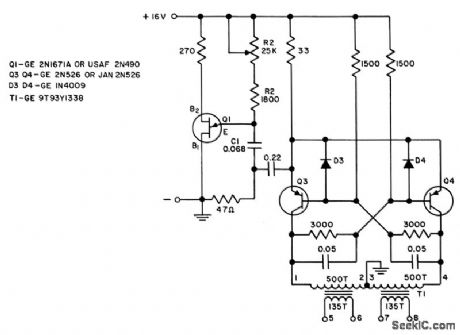
Uses transistor mvbr with unijunction transistor to stabilize and control frequency Efficiency is 85%. Has good fro. quency stability. Square-wave outputs are used lo drive d-c to a-c inverter. - Transistor Manual, Seventh Edition, General Electric Co., 1964, p 236. (View)
View full Circuit Diagram | Comments | Reading(1156)
TRANSFORMER_CONTROLLED__MVBR
Published:2009/7/15 5:06:00 Author:Jessie
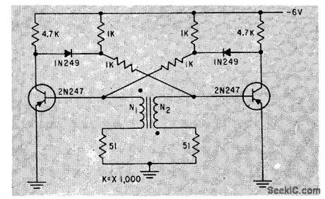
Gives sharper trailing edges und tighter control over ratio of on times of the two sides, as compared to choke control for same free-running mvbr. -W. M. Carey, Using Inductive Control in Computer Circuits, Electronics, 32:38, p 31-33. (View)
View full Circuit Diagram | Comments | Reading(525)
GATED_PULSE_TRAIN
Published:2009/7/15 21:00:00 Author:Jessie
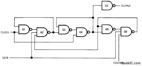
When control is logic 0, circuit transmits train of complete clock pulses to output, beginning with first clock pulse that starts to rise after application of gate signal and ending with last clock pulse that starts before gate signal falls. When control is logic 1, circuit transmits one complete clock pulse after logic 1 gate signal rises. To send another single pulse, gate signal must be removed and reapplied. Gates are Fairchild LPDT μL9047 triple three-input NAND and 9046 quad two-input NAND; other compatible DTL or TTL NAND gates can also be used.-J. V. Sastry, Gated Clock Generates Pulse Train or Single Pulse, EDN|EEE Magazine, July 1, 1971, p 50. (View)
View full Circuit Diagram | Comments | Reading(773)
PULSE_COUNTING_F_M_DISCRIMINATOR
Published:2009/7/15 21:00:00 Author:Jessie
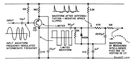
Based on inherent stability of tunnel diode as converter oscillator in f-m receiver for strong-signal locations. Uses 200-kc i-f center frequency as input,-D. Hubbard, Pulse Counter FM Discriminator Design, EEE, 10:7, p 44-49. (View)
View full Circuit Diagram | Comments | Reading(2175)
PRF_DISCRIMINATOR
Published:2009/7/15 20:58:00 Author:Jessie
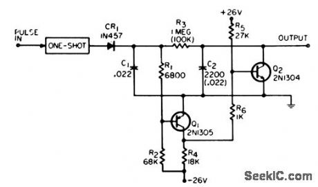
Requires pulse train burst of only two successive pulses to determine prf above or below given limit. Two such circuits with nand gate can indicate presence of given prf within 0.1% or within 1 cps of 1 kc. Input pulses are first given standard width and amplitude by one shot.-G. Richwell, PRF Discriminator, EEE, 13:7, p41. (View)
View full Circuit Diagram | Comments | Reading(658)
60_Hz_WITH_50_DUTY_CYCLE
Published:2009/7/15 20:57:00 Author:Jessie
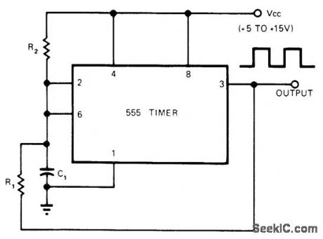
Adding single resistor R2 to standard oscillator connection of 555 timer permits operation with 50% duty cycle independently of frequency as determined by value of C1.For 60-Hz output, VCC is 10 V, C1 is 1 μF, R1 is 10K, and R2 is 75K.-R. Hofheimer, One Extra Resistor Gives 555 Timer 50% Duty Cycle, EDN Magazine, March 5, 1974, p 74-75. (View)
View full Circuit Diagram | Comments | Reading(3056)
DIGITAL_VOLTMETER_CALIBRATOR
Published:2009/7/14 2:48:00 Author:May
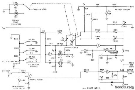
Calibration voltages of 100,10,and 1 V are derived from reference voltage, for use In calibrating digital voltmeter in which analog voltage is converted to pulse whose width is proportional to input amplitude.Used for gating clock pulses into digital counters for voltage readout.-B. Barker and M. McMahan,Digital Voltmeter Employs Voltage-To-Time Converter,Electronics,34:18, p 67-69. (View)
View full Circuit Diagram | Comments | Reading(635)
| Pages:157/471 At 20141142143144145146147148149150151152153154155156157158159160Under 20 |
Circuit Categories
power supply circuit
Amplifier Circuit
Basic Circuit
LED and Light Circuit
Sensor Circuit
Signal Processing
Electrical Equipment Circuit
Control Circuit
Remote Control Circuit
A/D-D/A Converter Circuit
Audio Circuit
Measuring and Test Circuit
Communication Circuit
Computer-Related Circuit
555 Circuit
Automotive Circuit
Repairing Circuit