
Circuit Diagram
Index 69
Linear Resistance Meter
Published:2013/7/24 20:24:00 Author:muriel | Keyword: Linear Resistance Meter

Most analogue multimeters are capable of measuring resistance over quite a wide range of values, but are rather inconvenient in use due to the reverse reading scale which is also non-linear. This can also give poor accuracy due to cramping of the scale that occurs at the high value end of each range. This resistance meter has 5 ranges and it has a forward reading linear scale on each range.The full-scale values of the 5 ranges are 1K, 10K, 100K, 1M &10M respectively and the unit is therefore capable of reasonably accurate measurements from a few tens of ohms to ten Megohms.
The CircuitMost linear scale resistance meters including the present design, work on the principle that if a resistance is fed from a constant current source the voltage developed across that resistance is proportional to its value. For example, if a 1K resistor is fed from a 1 mA current source from Ohm’s Law it can be calculated that 1 volt will be developed across the resistor (1000 Ohms divided by 0.001 amps = 1 volt). Using the same current and resistance values of 100 ohms and 10K gives voltages of 0.1volts (100 ohms / 0.001amps = 0.1volts) and 10 volts (10000 ohms / 0.001amps = 10 volts).Thus the voltage developed across the resistor is indeed proportional to its value, and a voltmeter used to measure this voltage can in fact be calibrated in resistance, and will have the desired forward reading linear scale. One slight complication is that the voltmeter must not take a significant current or this will alter the current fed to the test resistor and impair linearity. It is therefore necessary to use a high impedance voltmeter circuit.The full circuit diagram of the Linear Resistance Meter is given in Figure 1. The constant current generator is based on IC1a and Q1. R1, D1 and D2 form a simple form a simple voltage regulator circuit, which feeds a potential of just over 1.2 volts to the non-inverting input of IC1a. There is 100% negative feedback from the emitter of Q1 to the inverting input of IC1a so that Q1’s emitter is stabilised at the same potential as IC1a’s non-inverting input. In other words it is stabilised a little over 1.2 volts below the positive supply rail potential. S3a gives 5 switched emitter resistances for Q1, and therefore 5 switched emitter currents. S3b provides 5 reference resistors across T1 & T2 via S2 to set full-scale deflection on each range using VR1.As the emitter and collector currents of a high gain transistor such as a BC179 device used in the Q1 are virtually identical, this also gives 5 switched collector currents. By having 5 output currents, and the current reduced by a factor of 10 each time S3a is moved one step in a clockwise direction, the 5 required measuring ranges are obtained. R2 to R6 must be close tolerance types to ensure good accuracy on all ranges. The high impedance voltmeter section uses IC1b with 100% negative feedback from the output to the inverting input so that there is unity voltage gain from the non-inverting input to the output. The output of IC1b drives a simple voltmeter circuit using VR1 and M1, and the former is adjusted to give the correct full-scale resistance values.The CA3240E device used for IC1 is a dual op-amp having a MOS input stage and a class A output stage. These enable the device to operate with the inputs and outputs right down to the negative supply rail voltage. This is a very helpful feature in many circuits, including the present one as it enables a single supply rail to be used where a dual balanced supply would otherwise be needed. In many applications the negative supply is needed simply in order to permit the output of the op-amp to reach the 0volt rail. In applications of this type the CA3240E device normally enables the negative supply to be dispensed with.As the CA3240E has a MOS input stage for each section the input impedance is very high (about 1.5 million Megohms!) and obviously no significant input current flows into the device. This, together with the high quality of the constant current source, and the practically non-existent distortion through IC1b due to the high feedback level gives this circuit excellent linearity.With no resistor connected across T1 & T2 M1 will be taken beyond full-scale deflection and overloaded by about 100 or 200%. This is unlikely to damage the meter, but to be on the safe side a push-to-test on/off switch (S1) is used. Thus the power is only applied to the circuit when a test resistor is connected to the unit, and prolonged meter overloads are thus avoided.A small (PP3 size) 9 volt battery is a suitable power source for this project which has a current consumption of around 5mA and does not require a stabilised supply.
Photos showing inside and outside of the completed Linear Resistance Meter. (View)
View full Circuit Diagram | Comments | Reading(2554)
Beeper to find short circuits
Published:2013/7/23 21:20:00 Author:muriel | Keyword: Beeper , short circuits

This circuit uses two 741s or equivalent op amp to form a beeper that is used to detect short circuits. This design offers a way to trace resistance in the milliohm range, right to a short between bridged traces beneath a solder mask. A1 is configured as a multivibrator. R1 and C1 determine the frequency of oscillation and Q1 and Q2 boost the output. Assuming a virtual ground at the output of A2, free-run frequency is about 1kHz. Q1 and Q2 deliver a +/-10v squarewave to R4, dumping a +/-100mA through a short circuit placed across the probe tips. R5 ensures that the open circuit voltage never exceeds +/-0.1v. A2 monitors the voltage between the probes. When the probes are open, A2's gain equals the R4/R5 divider loss, and the output of both amplifiers is identical. This has two effects: First, hysteresis is greatly increased and frequency falls to a low growl, and secondly, the loudspeaker that bridges the two in-phase outputs is effectively silenced. A dead short across the probe tips will return nothing to A2 and the circuit will squeal at its nominal 1kHz rate. Anything less than a perfect short produces some output from A2, increasing multivibrator hysteresis and lowering the pitch.
(View)
View full Circuit Diagram | Comments | Reading(803)
Receiver circuit diagram
Published:2013/7/23 21:20:00 Author:muriel | Keyword: Receiver circuit diagram
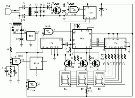
Receiver Parts:R1 100K 1/4W ResistorR2 1K 1/4W ResistorR3,R4,R6-R8 12K 1/4W ResistorsR5 47K 1/4W ResistorR9-R15 470R 1/4W ResistorsR16 680R 1/4W ResistorC1,C2 47nF 400V Polyester CapacitorsC3,C7 1nF 63V Polyester CapacitorsC4 10nF 63V Polyester CapacitorC5,C6,C10 220nF 63V Polyester CapacitorsC8 1000µF 25V Electrolytic CapacitorC9 100pF 63V Ceramic CapacitorD1,D2,D5 1N4148 75V 150mA DiodesD4,D4 1N4002 100V 1A DiodesD6-D8 Common-cathode 7-segment LED mini-displaysIC1 4093 Quad 2 input Schmitt NAND Gate ICIC2 4518 Dual BCD Up-Counter ICIC3 78L12 12V 100mA Voltage regulator ICIC4 4017 Decade Counter with 10 decoded outputs ICIC5 4553 Three-digit BCD Counter ICIC6 4511 BCD-to-7-Segment Latch/Decoder/Driver ICQ1 BC239C 25V 100mA NPN TransistorQ2-Q4 BC327 45V 800mA PNP TransistorsL1 Primary (Connected to C1 & C2): 10 turnsSecondary: 100 turnsWire diameter: O.2mm. enameledPlastic former with ferrite core. Outer diameter: 4mm. T1 220V Primary, 12+12V Secondary 3VA Mains transformerPL1 Male Mains plug & cable
Device purpose:This circuit is intended for precision centigrade temperature measurement, with a transmitter section converting to frequency the sensor's output voltage proportional to the measured temperature. The output frequency bursts are conveyed into the mains supply cables.The receiver section counts the bursts coming from mains supply and shows the counting on three 7-segment LED displays. The least significant digit displays tenths of degree and then a 00.0 to 99.9 °C range is obtained.Transmitter-receiver distance can reach hundred meters, provided both units are connected to the mains supply within the control of the same light-meter.
Transmitter circuit operation:IC1 is a precision centigrade temperature sensor with a linear output of 10mV/°C driving IC2, a voltage-frequency converter. At its output pin (3), an input of 10mV is converted to 100Hz frequency pulses. Thus, for example, a temperature of 20°C is converted by IC1 to 200mV and then by IC2 to 2KHz. Q1 is the driver of the power output transistor Q2, coupled to the mains supply by L1 and C7,C8.
Receiver circuit operation:The frequency pulses coming from mains supply and safely insulated by C1,C2 & L1 are amplified by Q1; diodes D1,D2 limiting peaks at its input. Pulses are filtered by C5, squared by IC1B, divided by 10 in IC2B and sent for the final count at the clock input of IC5.IC4 is the time-base generator: it provides reset pulses for IC1B and IC5 and enables latches and gate-time of IC5 at 1Hz frequency. It is driven by a 5Hz square wave obtained from 50Hz mains frequency picked-up from T1 secondary, squared by IC1C and divided by 10 in IC2A.IC5 drives the displays' cathodes via Q2,Q3 & Q4 at a multiplexing rate frequency fixed by C7. It drives also the 3 displays' paralleled anodes via the BCD-to-7 segment decoder IC6.Summing up, input pulses from mains supply at, say, 2KHz frequency, are divided by 10 and displayed as 20.0°C.
Notes:D6 is the Most Significant Digit and D8 is the Least Significant Digit.R16 is connected to the Dot anode of D7 to permanently light the decimal point.Set the ferrite cores of both inductors for maximum output (best measured with an oscilloscope, but not critical).Set trimmer R4 in the transmitter to obtain a frequency of 5KHz at pin 3 of IC2 with an input of 0.5Vcc at pin 7 (a digital frequency meter is required).More simple setup: place a thermometer close to IC1 sensor, then set R4 to obtain the same reading of the thermometer in the receiver's display.Keep the sensor (IC1) well away from heating sources (e.g. Mains Transformer T1).Linearity is very good.
(View)
View full Circuit Diagram | Comments | Reading(713)
Digital Remote Thermometers
Published:2013/7/23 21:19:00 Author:muriel | Keyword: Digital Remote Thermometers

Transmitter parts:R1,R3 100K 1/4W ResistorsR2 47R 1/4W ResistorR4 5K 1/2W Trimmer CermetR5 12K 1/4W ResistorR6 10K 1/4W ResistorR7 6K8 1/4W ResistorR8,R9 1K 1/4W ResistorsC1 220nF 63V Polyester CapacitorC2 10nF 63V Polyester CapacitorC3 1µF 63V Polyester CapacitorC4,C6 1nF 63V Polyester CapacitorsC5 2n2 63V Polyester CapacitorC7,C8 47nF 400V Polyester CapacitorsC9 1000µF 25V Electrolytic CapacitorD1 1N4148 75V 150mA DiodeD2,D3 1N4002 100V 1A DiodesD4 5mm. Red LEDIC1 LM35 Linear temperature sensor ICIC2 LM331 Voltage-frequency converter ICIC3 78L06 6V 100mA Voltage regulator ICQ1 BC238 25V 100mA NPN TransistorQ2 BD139 80V 1.5A NPN TransistorL1 Primary (Connected to Q2 Collector): 100 turnsSecondary: 10 turnsWire diameter: O.2mm. enameledPlastic former with ferrite core. Outer diameter: 4mm. T1 220V Primary, 12+12V Secondary 3VA Mains transformerPL1 Male Mains plug & cable (View)
View full Circuit Diagram | Comments | Reading(1317)
Mosfet TESTER
Published:2013/7/23 21:19:00 Author:muriel | Keyword: Mosfet TESTER
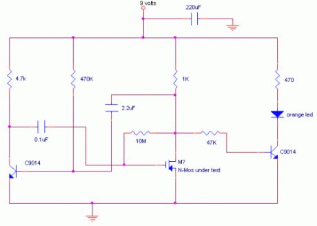
This is a variation on the astable multivibrator. Circuit was recently developed to test for N-mosfets(the power kind e.g irf830)I don’t claim circuit can test all bad mosfets or all fault mosfet conditions. If mosfet is working it will operate in the astable multivibrator circuit causing the Led to flash.A bad mosfet will not cause the LED to flash.Below is the circuit diagram, the other half of the astable utilizes an npn transistor to make the circuit cheap.Almost any npn transistor will work in this circuit.The npn transistor to the right is used as a common emitter buffer that also drives the led as it receives pulses from the mosfet drain. (View)
View full Circuit Diagram | Comments | Reading(1792)
Continuity Tester
Published:2013/7/23 21:18:00 Author:muriel | Keyword: Continuity Tester
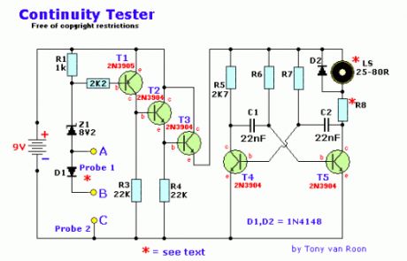
PartsR1 1K R2 2K2 R3,R4 22K R5 2K7 R6,R7 56K R8 *See text C1,C2 22nF D1,D2 1N4148Z1 8V2, 1/4 wattT1 2N3905 (PNP)T2,3,4,5 2N3904 (NPN)9volt Alkaline batterysuitable loudspeakerhousing & probes
An on-off switch is unnecessary. D1 is used when the batteryis brand-new and giving over the nominal 9volt, T1, T2 and T3 acting as the switch for supplying power to the multivibrator.
Design Considerations:Several simple circuits were tried -- a lamp, battery and probes still demanded the attention of the eyes; replacing the lamp with a buzzer was more successful but needed some three to four volts and gave no indication of a series semiconductor junction if the polarity was correct while the current flow was large enough to damage the more delicate devices within the circuit under test. An extension of the principle to operate an astable (multivibrator) type of oscillator gave good audibility but would operate from zero through to several thousands of ohms and so was too general an indication.A set of specification was becoming apparent; (1) probe current to be small; (2) probe voltage to be as low as possible, preferable less than 0.3V to avoid seeing germanium or silicon junctions as a continuous circuit; (3) no on/off switch to be used.The above circuit was the result and several have been designed and are earning their keep for both heavy electricians and electronic technicians.
(View)
View full Circuit Diagram | Comments | Reading(0)
Transistor Testers
Published:2013/7/23 21:17:00 Author:muriel | Keyword: Transistor Testers
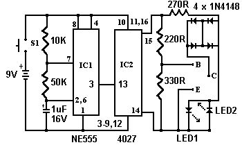
This simple circuit has helped me out on many occasions. It is able to check transistors, in the circuit, down to 40 ohms across the collector-base or base-emitter junctions. It can also check the output power transistors on amplifier circuits.Circuit operation is as follows. The 555 timer ( IC1 ) is set up as a 12hz multi vibrator. The output on pin 3 drives the 4027 flip-flop (IC2). This flip-flop divides the input frequency by two and delivers complementary voltage outputs to pin 15 and 14. The outputs are connected to LED1 and LED2 through the current limiting resistor R3. The LED's are arranged so that when the polarity across the circuit is one way only one LED will light and when the polarity reverses the other LED will light, therefore when no transistor is connected to the tester the LED's will alternately flash. The IC2 outputs are also connected to resistors R4 and R5 with the junction of these two resistors connected to the base of the transistor being tested. With a good transistor connected to the tester, the transistor will turn on and produce a short across the LED pair. If a good NPN transistor is connected then LED1 will flash by itself and if a good PNP transistor is connected then LED2 will flash by itself. If the transistor is open both LED's will flash and if the transistor is shorted then neither LED will flash.
(View)
View full Circuit Diagram | Comments | Reading(1261)
Capacitance Meter
Published:2013/7/23 21:17:00 Author:muriel | Keyword: Capacitance Meter
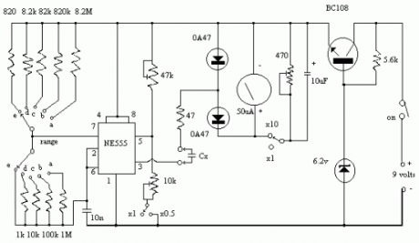
Position Range a 1 ufb 100 nfc 10 nfd 1 nfe 100 pfUse X10 switch to measure up 10uf.Use X0.5 switch for better readings on low values.
This project is more complex than the others described earlier. However, when finished, you will have an instrument capable of measuring all but the largest capacitors used in radio circuits. Unlike variable resistors, most variable capacitors are not marked with their values. As well, the markings of capacitors from salvaged equipment often rub off. By being able to measure these unmarked components, this project will prove useful to the constructor, vintage radio enthusiast or antenna experimenter.The common 555 timer IC forms the heart of the circuit (Figure Three). Its function is to charge the unknown capacitor (Cx) to a fixed voltage. The capacitor is then discharged into the meter circuit. The meter measures the current being drawn through the 47 ohm resistor. The 555 repeats the process several times a second, so that the meter needle remains steady.The deflection on the meter is directly proportional to the value of the unknown capacitor. This means that the scale is linear, like the voltage and current ranges on an analogue multimeter.The meter has five ranges, from 100pF to 1uF, selected by a five position two pole switch. In addition, there is a x10 switch for measuring higher values and a divide-by-two facility to allow a better indication on the meter where the capacitor being measured is just above 100, 1000pF, 0.01, 0.1 or 1 uF.Component values are critical. For best accuracy, it is desirable that the nine resistors wired to the Range switch have a 2% tolerance. If 0A47 diodes are not available, try OA91 or OA95 germanium diodes instead. Construct the meter in a plastic box; one that is about the size of your multimeter but deeper is ideal. The meter movement should as large as your budget allows; you will be using it to indicate exact values. A round 70mm-diameter movement salvaged from a piece of electronic equipment was used in the prototype. The meter you buy will have a scale of 0 to 50 microamps. This scale needs to be converted to read 0 to 100 (ie 20, 40, 60, 80, 100 instead of 10, 20, 30, 40, 50). Use of white correction fluid or small pieces of paper will help here.The components can be mounted on a piece of matrix board or printed circuit board. Use a socket for the IC should replacement ever be needed. Keep wires short to minimise stray capacitance; stray capacitance reduces accuracy.Calibrating the completed meter can be done in conjunction with a ready-built capacitance meter. Failing this, a selection of capacitors of known value, as measured on a laboratory meter, could be used. If neither of these options are available, simply buy several capacitors of the same value and use the one which is nearest the average as your standard reference. Use several standards to verify accuracy on all ranges.To calibrate, disable both the x10 and divide-by-two functions (ie both switches open). Then connect one of your reference capacitors and switch to an appropriate range. Vary the setting of the 47k trimpot until the meter is reading the exact value of the capacitor. Then switch in the divide-by-two function. This should change the reading on the meter. Adjust the 10k trimpot so that the needle shows exactly twice the original reading. For example, if you used a 0.01 uF reference, and the meter read 10 on the 0.1 uF range, it should now read 20. Now switch out the divide-by-two function.If you are not doing so already, change to a reference with a value equal to one of the ranges (eg 1000pF, 0.01uF, 0.1uF etc). Switch to the range equal to that value (ie the meter reads full-scale (100) when that capacitor is being measured. Switching in the x10 function should cause the meter indication to drop significantly. Adjust the 470 ohm trimpot so that the meter reads 10. Move down one range (eg from 0.01uF to 1000pF). The meter should read 100 again. If it does not, vary the 470 ohm trimpot until it does. That completes the calibration of the capacitance meter. Now try measuring other components to confirm that the measurements are reasonable.With care, an accuracy of five percent or better should be possible on most ranges.
(View)
View full Circuit Diagram | Comments | Reading(0)
Digital Radar Speedometers
Published:2013/7/23 21:16:00 Author:muriel | Keyword: Digital Radar Speedometers

This circuit is a Digital Radar Speedometer. It allows us to evaluate the speed of any object moving, especially cars and other vehicles. The speed is calculated in kilometers per hour (KPH). Its display has three digits. This radar works with the laser reflexion. It sends laser radiation to the object and this object reflects the laser radiation to the radar. To evaluate the speed of a vehicle, we must be in front of it. In other words, the vehicle must come in our direction. The front of the radar must point the front of the vehicle. The radar has the shape of a pistol. In this radar, it has a laser LED and a laser diode. Both have a lens.The laser LED can send a spot of light to a distance of 90 m (295 ft). It's very important that the distance range of the laser LED is 90 m, if not, the speed will not be calculated properly. The laser diode, which receives the light signal by the laser LED, must be able to detect the light which is same color as that emitted by the laser LED. The laser diode and the laser LED must be placed one beside the other. They are protected by a tinted pane. They must be placed at the front of the radar and point the outside. The radar is powered by a 9V battery and it has a SPST switch to control its power state.The display, or the speed indicator, is placed at the rear of the radar, just on the right of the overload LED indicator. All the logic components of the circuit must be of the 74AS series and TTL type. Because they have short time of response (less than 1.7 ns) and have high frequency supports (more than 200 MHz). The radar can evaluate the speed of an object moving between 0 to 999 km/h. After this speed, the overload LED indicator will turn on and the 999 will still displayed. The radar displays the speed during 3 seconds, after this time, it displays zero (0).
(View)
View full Circuit Diagram | Comments | Reading(1880)
Sample Power Supply 2
Published:2013/7/23 21:15:00 Author:muriel | Keyword: Sample Power Supply

View full Circuit Diagram | Comments | Reading(887)
Sample Power supply 1
Published:2013/7/23 21:15:00 Author:muriel | Keyword: Sample Power supply

View full Circuit Diagram | Comments | Reading(2098)
Led display digital Voltmeter
Published:2013/7/23 21:14:00 Author:muriel | Keyword: Led display, digital Voltmeter
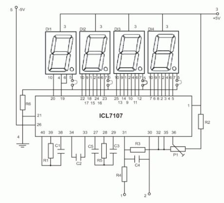
This is an easy to build, but nevertheless very accurate and useful digital voltmeter. It has been designed as a panel meter and can be used in DC power supplies or anywhere else it is necessary to have an accurate indication of the voltage present. The circuit employs the ADC (Analogue to Digital Converter) I.C. CL7107 made by INTERSIL. This IC incorporates in a 40 pin case all the circuitry necessary to convert an analogue signal to digital and can drive a series of four seven segment LED displays directly. The circuits built into the IC are an analogue to digital converter, a comparator, a clock, a decoder and a seven segment LED display driver. The circuit as it is described here can display any DC voltage in the range of 0-1999 Volts.
Technical Specifications - CharacteristicsSupply Voltage: ............. +/- 5 V (Symmetrical)Power requirements: ..... 200 mA (maximum)Measuring range: .......... +/- 0-1,999 VDC in four rangesAccuracy: ....................... 0.1 %FEATURES- Small size- Easy construction- Low cost.- Simple adjustment.- Easy to read from a distance.- Few external components.
How it WorksIn order to understand the principle of operation of the circuit it is necessary to explain how the ADC IC works. This IC has the following very important features:- Great accuracy.- It is not affected by noise.- No need for a sample and hold circuit.- It has a built-in clock.- It has no need for high accuracy external components.
(View)
View full Circuit Diagram | Comments | Reading(2251)
Digital Voltmeter
Published:2013/7/23 21:13:00 Author:muriel | Keyword: Digital Voltmeter
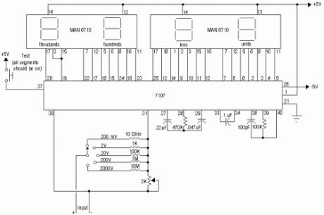
The ICL7107 is a 3 1/2 digit LED A/D convertor. It contains an internal voltage reference, high isolation analog switches, sequential control logic, and the display drivers. The auto-zero adjust ensures zero reading for 0 volts input.
(View)
View full Circuit Diagram | Comments | Reading(1989)
Brightness Control for small Lamp
Published:2013/7/23 21:12:00 Author:muriel | Keyword: Brightness Control, small Lamp
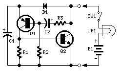
Parts:P1 470K Linear PotentiometerR1 10K 1/4W ResistorR2 47K 1/4W Resistor (See Notes)R3 1K5 1/4W ResistorC1 22nF 63V Polyester CapacitorC2 100µF 25V Electrolytic CapacitorD1,D2 1N4148 75V 150mA DiodesIC1 7555 or TS555CN CMos Timer ICQ1 BD681 100V 4A NPN Darlington TransistorLP1 1.5V 200mA Bulb (See Notes)SW1 SPST SwitchB1 3V (Two 1.5V AA or AAA cells in series, etc.)
Circuit operation:This device was designed on request, to control the light intensity of four filament lamps (i.e. a ring illuminator) for close-up pictures with a digital camera, powered by two AA or AAA batteries. Obviously it can be used in other ways, at anyone's will.IC1 generates a 150Hz squarewave having a variable duty-cycle. When the cursor of P1 is fully rotated towards D1, the output positive pulses appearing at pin 3 of IC1 are very narrow. Lamp LP1, driven by Q1, is off as the voltage across its leads is too low. When the cursor of P1 is rotated towards R2, the output pulses increase in width, reaching their maximum amplitude when the potentiometer is rotated fully clockwise. In this way the lamp reaches its full brightness.
Notes:LP1 could be one or more 1.5V bulbs wired in parallel. Maximum total output current allowed is about 1A.R2 limits the output voltage, measured across LP1 leads, to 1.5V. Its actual value is dependent on the total current drawn by the bulb(s) and should be set at full load in order to obtain about 1.5V across the bulb(s) leads when P1 is rotated fully clockwise.
(View)
View full Circuit Diagram | Comments | Reading(945)
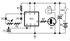
The flashing Heart
Published:2013/7/23 21:12:00 Author:muriel | Keyword: The flashing Heart

The Circuit Diagram is shown in Figure 1. It consists of a 4047 low-power monostable/astable multivibrator, IC1, used in the astable mode to provide the timing pulses to control the flash rate of the LEDs. To accomplish the astable mode, pins 4, 5, 6, and 14 are connected to +12VDC and pins 7, 8, 9, and 12 are connected to ground. Pins 1 and 3 are connected to C2 and pins 2 and 3 are connected to potentiometer R9. A fixed value resistor can be used in place of the potentiometer R9, if the flash rate does not need to be adjusted. These three pins make up the R-C timing circuit. The output pulses from the 4047 are taken from pins 10, 11, and 13. Pin 10 is the Q output and pin 11 is the Q-not output. These two pins are onnected to R6 and R7 respectively.
The collectors of Q2 and Q3 are connected to R4 and R5 respectively, which are connected to the cathodes of the Yellow LEDs. Pin 13 is the oscillator output and is connected to R8, which is connected to the base of Q1. The collector of Q1 is connected to R3, which is connected to the cathodes of the Red LED's. The emitters of the three transistors are connected to ground. The Green LEDs are connected to R1 and R2, which are connected to +12VDC. Resistors R1-R8 are current limiting resistors and the correct wattage for these resistors should be used to prevent excessive heat. The resistive values may be changed to vary the brightness of the LEDs. The circuit is powered by PS1, a wall transformer, which is connected to a filter capacitor C1. It must be between 10 to 15 VDC and at least 500mA.
ConstructionProbably the most difficult part of this project is making the printed circuit board, Figure 2. The board used in the prototype took several hours to make using dry transfers. Using a different technique, such as photo resist, may be faster for the experienced hobbyist. Once the board is etched and drilled, the jumper wires should be placed on the board and soldered, as shown on Figure 3. Next the 84 Yellow LEDs should be placed around the border of the board, followed by the 42 Red LEDs that make up the heart and then the 16 Green LEDs that make up the letters I and U. Resistors R1-R9 and capacitors C1and C2 should be placed on the board next and then the power supply, PS1. Sockets were used in the prototype for the I.C. and transistors. A socket for the I.C. is required, but the sockets for the transistors are not. Special care should be taken when handling the CMOS I.C., as a static discharge will destroy it. When you are finished soldering, check the board over for mistakes. If everything looks okay, apply power. (View)
View full Circuit Diagram | Comments | Reading(1232)
Fading LED
Published:2013/7/23 21:09:00 Author:muriel | Keyword: Fading LED
Parts:R1,R2 4K7 1/4W ResistorsR3 22K 1/4W ResistorR4 1M 1/4W Resistor (See Notes)R5 2M2 1/4W Carbon Trimmer (See Notes)R6,R10,R11,R14,R15 10K 1/4W ResistorsR7,R8 47K 1/4W Carbon Trimmers (See Notes)R9,R13 27K 1/4W ResistorsR12,R16 56R 1/4W ResistorsC1 1µF 63V Polyester CapacitorC2 100µF 25V Electrolytic CapacitorD1-D4 etc 5 or 3mm. LEDs (any type and color) (See Notes)IC1 LM358 Low Power Dual Op-ampQ1,Q2,Q4 BC327 45V 800mA PNP TransistorsQ3,Q5,Q6 BC337 45V 800mA NPN TransistorsSW1 SPST miniature Slider SwitchB1 9V PP3 BatteryClip for PP3 Battery
Device purpose:This circuit operates two LED strips in pulsing mode, i.e. one LED strip goes from off state, lights up gradually, then dims gradually, etc. while the other LED strip do the contrary.Each strip can be made up from 2 to 5 LEDs at 9V supply.
Circuit operation:The two Op-Amps contained into IC1 form a triangular wave generator. The rising and falling voltage obtained at pin #7 of IC1 drives two complementary circuits formed by a 10mA constant current source (Q1, Q2 and Q5, Q6) and driver transistor (Q3 and Q6).R4, R5 & C1 are the timing components: the total period can be varied changing their values. R7 & R8 vary the LEDs brightness.
Notes:For those whishing to avoid the use of trimmers, suggested values for a 9V supply are:R4=3M9, R9 & R13=47K and trimmers replaced by a short.Whishing to use a wall-plug transformer-supply instead of a 9V battery, you can supply the circuit at 12V, allowing the use of up to 6 LEDs per strip, or at 15V, allowing the use of up to 7 LEDs per strip.In this case, the value of the trimmers R7 & R8 should be changed to 100K.
(View)
View full Circuit Diagram | Comments | Reading(1272)
LEDs or Lamps Sequencer
Published:2013/7/23 21:08:00 Author:muriel | Keyword: LEDs, Lamps, Sequencer

Parts:R1 1K5 1/4W ResistorR2 680R 1/4W Resistor (Optional, see text)C1 47µF 25V Electrolytic CapacitorD1 LED any typeQ1 BC337 45V 800mA NPN TransistorP1 SPST PushbuttonLP1 Filament Lamp 12 or 24V (See text)
Comments:The purpose of this circuit was to create a ring in which LEDs or Lamps illuminate sequentially. Its main feature is a high versatility: you can build a loop containing any number of LEDs or Lamps, as each illuminating device has its own small circuit.The diagrams show three-stage circuits for simplicity: you can add an unlimited number of stages (shown in dashed boxes), provided the last stage output was returned to the first stage input, as shown.P1 pushbutton purpose is to allow a sure start of the sequence at power-on but, when a high number of stages is used, it also allows illumination of more than one LED or Lamp at a time, e.g. one device illuminated and three out and so on.After power-on, P1 should be held closed until only the LED or Lamp related to the module to which the pushbutton is connected remains steady illuminated. When P1 is released the sequencer starts: if P1 is pushed briefly after the sequence is started, several types of sequence can be obtained, depending from the total number of stages.
Notes:If one LED per module is used, voltage supply can range from 6 to 15V.You can use several LEDs per module. They must be wired in series and supply voltage must be related to their number.Using 24V supply (the maximum permitted voltage), about 10 LEDs wired in series can be connected to each module, about 7 at 15V and no more than 5 at 12V.The right number of LEDs can vary, as it is depending by their color and brightness required.Using lamps, voltage supply can range from 9 to 24V. Obviously, lamp voltage must be the same of supply voltage.In any case, lamps may also be wired in series, e.g. four 6V lamps wired in series can be connected to each module and powered by 24V supply.If you intend to use lamps drawing more than 400mA current, BC337 transistors should be substituted by Darlington types like BD677, BD679, BD681, 2N6037, 2N6038, 2N6039 etc.As Darlington transistor usually have a built-in Base-Emitter resistor, R1 may be omitted, further reducing parts counting.Sequencer speed can be varied changing C1 value.A similar design appeared in print about forty years ago. It used germanium transistors and low voltage lamps. I think the use of LEDs, silicon transistors, Darlington transistors and 24V supply an interesting improvement. (View)
View full Circuit Diagram | Comments | Reading(1394)
Instrument panel lamp dimmer control
Published:2013/7/23 21:07:00 Author:muriel | Keyword: Instrument panel, lamp dimmer , control
This circuit uses an MC3392 low side protected switch and an MC1455 timing circuit to form an automotive instrumentation panel lamp dimmer control. The brightness of incandescent lamps can be varied by Pulse Width Modulating the input of the MC3392. The modulating signal can be obtained directly from the MC1455 timer (or a microprocessor). The MC1455 is configured as a free-running clock having a frequency and duty cycle control. The typical timer frequency is approximately 80 Hz when the frequency potentiometer is adjusted to 1.0k. This frequency was chosen so as to avoid any perceptible lamp flicker. The duty cycle potentiometer controls the duty cycle over a range of about 3% to 97%. When at 3% the lamps are essentialy off, at 97% the lamps are essentially full on. Any number of lamps can be control, so long as the total load current is less than 1 amp. The LED is used to signal the existence of a system fault (overvoltage, current limiting, or thermal shutdown). (View)
View full Circuit Diagram | Comments | Reading(1021)
Bicycle back Safety Lights
Published:2013/7/23 21:05:00 Author:muriel | Keyword: Bicycle back, Safety Lights
Parts:R1 10K 1/4W ResistorR2,R9,R10 100K 1/4W ResistorsR3-R8,R11-R16 10R 1/4W ResistorsR17 150R 1/4W ResistorC1 1µF 63V Polyester CapacitorC2 10nF 63V Polyester CapacitorC3 100µF 25V Electrolytic CapacitorD1-D13 Red LEDs 5mm. or bigger, high efficiencyIC1,IC2 7555 or TS555CN CMos Timer ICSW1 SPST Slider SwitchB1 3V Battery (2 AA 1.5V Cells in series)
Device purpose:This circuit has been designed to provide a clearly visible light, formed by 13 high efficiency flashing LEDs arranged in a pseudo-rotating order. Due to low voltage, low drain battery operation and small size, the device is suitable for mounting on bicycles as a back light, or to put on by jogger/walkers.
Circuit operation:IC1 is a CMos version of the 555 IC wired as an astable multivibrator generating a 50% duty-cycle square wave at approx. 4Hz frequency. At 3V supply, 555 output (pin 3) sinking current operation is far better than sourcing, then LED D1-D6 are connected to positive supply. In order to obtain an alternate flashing operation, a second 555 IC is provided, acting as a trigger plus inverter and driving LEDs D7-D12. D13 is permanently on.The LEDs are arranged in a two series display as shown below, with a center LED permanently on. This arrangement and the alternate flashing of the two series of LEDs provide a pseudo-rotating appearance.
(View)
View full Circuit Diagram | Comments | Reading(1107)
Two-wire Lamp Flashers
Published:2013/7/23 21:04:00 Author:muriel | Keyword: Two-wire, Lamp Flashers
Parts:R1 6K8 1/4W ResistorR2 270K 1/4W ResistorR3 22K 1/4W ResistorC1 220µF 25V Electrolytic CapacitorC2 10µF 25V Electrolytic CapacitorD1 1N4002 100V 1A DiodeQ1 BC557 45V 100mA PNP TransistorQ2 BD139 80V 1.5A NPN TransistorLP1 Existing filament Lamp: any type in the range 3-24V 10W max.SW1 Existing On-Off switchB1 Existing V DC source: any type in the range 3-24Vsuited to the lamp adopted
Device purpose:This circuit has been designed to provide that continuous light lamps already wired into a circuit, become flashing. Simply insert the circuit between existing lamp and negative supply.Especially suited for car or panel pilot lights, this device can drive lamps up to 10W.
Notes:Break lamp(s) to negative supply connection(s), then insert the circuit between existing lamp(s) connection(s) and negative supply (respecting polarities!).C1 value can be varied from 100 to 1000µF or higher, in order to change flashing frequency.Although rather oversized, this circuit can also drive any LED, providing a suitable resistor is fitted in series with the light emitting device.The resistor should be in the range 47R to 2K2, depending on supply voltage
(View)
View full Circuit Diagram | Comments | Reading(1293)
| Pages:69/2234 At 206162636465666768697071727374757677787980Under 20 |
Circuit Categories
power supply circuit
Amplifier Circuit
Basic Circuit
LED and Light Circuit
Sensor Circuit
Signal Processing
Electrical Equipment Circuit
Control Circuit
Remote Control Circuit
A/D-D/A Converter Circuit
Audio Circuit
Measuring and Test Circuit
Communication Circuit
Computer-Related Circuit
555 Circuit
Automotive Circuit
Repairing Circuit