
Circuit Diagram
Index 70
Lamp Pulser
Published:2013/7/23 21:03:00 Author:muriel | Keyword: Lamp Pulser

Parts:R1,R2 4K7 1/4W ResistorsR3 22K 1/4W ResistorR4 2M2 1/4W Resistor (See Notes)R5 10K 1/4W ResistorR6 47R 1/4W Resistor (See Notes)C1 1µF 63V Polyester CapacitorD1 5mm. Red LED (See Notes)IC1 LM358 Low Power Dual Op-ampQ1 BC337 45V 800mA NPN Transistor
Circuit operation:This circuit operates a LED in pulsing mode, i.e. the LED goes from off state, lights up gradually, then dims gradually, etc.This operation mode is obtained by a triangular wave generator formed by two op-amps contained in a very cheap 8 pin DIL case IC. Q1 ensures current buffering, in order to obtain a better load drive.R4 & C1 are the timing components: using the values shown in the parts list, the total period is about 4 seconds.
Notes:The most satisfying results are obtained adopting for R4 a value ranging from 220K to 4M7.Adopting for R4 a value below 220K, the pulsing effect will be indistinguishable from a normal blinking effect.The LED can be any type and color.You can use a filament lamp instead, provided its features are comprised in the range 3.2 to 6V, 200mA max.Using a lamp as a load, R6 must be omitted.Voltage supply range can be 4 to 6V: 4.5V is the best compromise.Don't supply the circuit with voltages exceeding 6V: it will work less good and Q1 could be damaged when a lamp was used as the load.At 6V supply, increase R6 value to 100 Ohm. (View)
View full Circuit Diagram | Comments | Reading(1096)
Dancing LED
Published:2013/7/22 20:15:00 Author:muriel | Keyword: Dancing LED
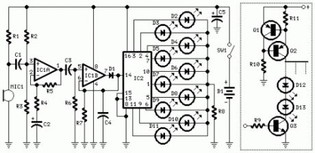
Parts:R1 10K 1/4W ResistorR2,R3 47K 1/4W ResistorsR4 1K 1/4W ResistorR5,R6,R7 100K 1/4W ResistorsR8 820R 1/4W ResistorC1,C3 100nF 63V Ceramic or Polyester CapacitorsC2 10µF 50V Electrolytic CapacitorC4 330nF 63V Polyester Capacitor (See Notes)C5 100µF 25V Electrolytic CapacitorD1 1N4148 75V 150mA DiodeD2-D11 5 or 3mm. LEDs (any type and color)IC1 LM358 Low Power Dual Op-ampIC2 4017 Decade counter with 10 decoded outputs ICM1 Miniature electret microphoneSW1 SPST miniature Slider SwitchB1 9V PP3 BatteryClip for PP3 BatteryAdditional circuit parts (see Notes):R9,R10 10K 1/4W ResistorsR11 56R 1/4W ResistorD12,D13 etc 5 or 3mm. LEDs (any type and color)Q1,Q2 BC327 45V 800mA PNP TransistorsQ3 BC337 45V 800mA NPN Transistor
Device purpose:The basic circuit illuminates up to ten LEDs in sequence, following the rhythm of music or speech picked-up by a small microphone. The expanded version can drive up to ten strips, formed by up to five LEDs each, at 9V supply.
Circuit operation:IC1A amplifies about 100 times the audio signal picked-up by the microphone and drives IC1B acting as peak-voltage detector. Its output peaks are synchronous with the peaks of the input signal and clock IC2, a ring decade counter capable of driving up to ten LEDs in sequence.An additional circuit allows the driving of up to ten strips, made up by five LEDs each (max.), at 9V supply. It is formed by a 10mA constant current source (Q1 & Q2) common to all LED strips and by a switching transistor (Q3), driving a strip obtained from 2 to 5 series-connected LEDs. Therefore one transistor and its Base resistor are required to drive each strip used.
Notes:The sensitivity of the circuit can be varied changing R4 value.C4 value can be varied from 220 to 470nF in order to change the circuit speed-response to music peaks.Adopting the additional circuit, only one item for R10, R11, Q1 and Q2 is required to drive up to ten LED strips. On the contrary, one item of R9 and Q3 is necessary to drive each strip you decided to use.Each R9 input must be connected to IC2 output pins, in place of the LEDs D2-D11 shown. R8 must also be omitted.Whishing to use a lower number of LEDs or LED strips, pin #15 of IC2 must be disconnected from ground and connected to the first unused output pin. Example:if you decided to use 5 LEDs, pin #15 of IC2 must be connected to pin #1; if you decided to use 8 LEDs, pin #15 of IC2 must be connected to pin #9 etc.Current drawing of the circuit is about 10mA.Whishing to use a wall-plug transformer-supply instead of a 9V battery, you can supply the circuit at 12V, allowing the use of up to 6 LEDs per strip, or at 15V, allowing the use of up to 7 LEDs per strip.
(View)
View full Circuit Diagram | Comments | Reading(1225)
Triple Stroboscope
Published:2013/7/22 20:14:00 Author:muriel | Keyword: Triple Stroboscope

This circuit enables observation of movement between other stroboscopes. Generation of rectangular signal is based on NE555. This circuit requires a low power supply that is made from a simple transformer TR1, traditional rectifier bridge and zener diode.NE555 works in multivibrator mode generating astable pulses of 2Hz to 20Hz.The frequency is adjusted by potentiometer P1. The control potentiometer P1 can be placed as far as 30 meters away, for suspension of stroboscope’s work from far away.It is east to find all parts with facility in every electronic store, but it may be difficult to find the transformers TR2, TR3, TR4.Take extreme care handling this circuit because near C5-C7-C9 high voltages are present.
PartsR1 = 6,8 kR2 = 5,6 kR3 = 330R4,R6,R8 = 270 / 5 WR5,R7,R9 = 220 kP1 = 100 k linear potentiometerC1 = 100 uF / 16 VC2 = 4,7 uF / 16 VC3 = 10 nFC4,C6,C8 = 22 nF / 400 V, MKSC5,C7,C9 = 10 uF / 350 V, electrolytic (high quality)TR1 = Ordinary transformer 230 V / 9 V, 1,5 VATR2,TR3,TR4 = stroboscope transformer np (ZTK200)D1,D2,D3,D4 = 1N4149D5 = BZX85V Zener 3.9D6,D7,D8,D9,D10,D11 = 1N4004IO1 = NE555IO2,IO3,IO4 = MOC3020XE1,XE2,XE3 = stroboscope lamps FT50F1 = Fuse 0.8 A, 20 mmK1,K5 = connectors ARK200-2K2,K3,K4 = connectors ARK200-3S1 = Switch
(View)
View full Circuit Diagram | Comments | Reading(1209)
Knightrider lights for model cars
Published:2013/7/22 20:13:00 Author:muriel | Keyword: Knightrider lights, model cars
This simple circuit drives 6 LEDs in 'Knightrider scanner mode'. Power consumption depends mainly on the type of LEDs used if you use a 7555 (555 CMOS version).
Note that VDD and GND for the ICs are not shown in the circuit drawing.Pin-outs:(7)555 1 GND 2 TRIGGER 3 OUTPUT 4 RESET 5 CONTROL VOLTAGE 6 THRESHOLD 7 DISCHARGE 8 VDD 40171 Q5 2 Q1 3 Q0 4 Q2 5 Q6 6 Q7 7 Q3 8 GND 9 Q810 Q411 Q912 CO13 NOT ENABLE14 CLK15 RESET16 VDD (View)
View full Circuit Diagram | Comments | Reading(1442)
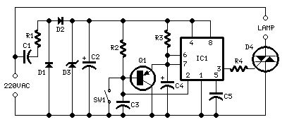
220 Volts Flashing Lamp
Published:2013/7/22 20:13:00 Author:muriel | Keyword: 220 Volts , Flashing Lamp

Parts:R1 100K 1/4W ResistorR2,R5 1K 1/4W ResistorsR3,R6 470R 1/4W ResistorsR4 12K 1/4W ResistorC1 1000µF 25V Electrolytic CapacitorD1-D4 1N4007 1000V 1A DiodesD5 P0102D 400V 800mA SCRQ1 BC327 45V 800mA PNP TransistorQ2 BC337 45V 800mA NPN TransistorPL1 Male Mains plugSK1 Female Mains socket
Device purpose:This circuit is intended as a reliable replacement to thermally-activated switches used for Christmas tree lamp-flashing. The device formed by Q1, Q2 and related resistors triggers the SCR. Timing is provided by R1,R2 & C1. To change flashing frequency don't modify R1 and R2 values: set C1 value from 100 to 2200µF instead.Best performances are obtained with C1=470 or 1000µF and R4=12K or 10K. Due to low consumption of normal 10 or 20 lamp series-loops intended for Christmas trees (60mA @ 220V typical for a 20 lamp series-loop), very small and cheap SCR devices can be used, e.g. C106D1 (400V 3.2A) or TICP106D (400V 2A), this last and the suggested P0102D devices having TO92 case.
Important Note:For proper operation it's absolutely necessary to employ high Gate-sensitive SCRs.If you are unable to find these devices you can use Triacs instead. In this case the circuit operates also with relatively powerful devices. A recommended Triac type is the ubiquitous TIC206M (600V 4A) but many others can work.Note that in spite of the Triac, diode bridge D1-D4 is in any case necessary.
This circuit was awarded with publication in ELECTRONICS WORLD Circuit Ideas , June 2000 issue, page 458
(View)
View full Circuit Diagram | Comments | Reading(1216)
Battery-powered Night Lamp 1
Published:2013/7/22 20:12:00 Author:muriel | Keyword: Battery-powered , Night Lamp

Parts:R1,R2 1M 1/4W ResistorsR3 47K 1/4W Resistor (optional: see Notes)R4 Photo resistor (any type, optional: see Notes)C1 100nF 63V Polyester CapacitorC2 220µF 25V Electrolytic CapacitorD1 LED Red 10mm. Ultra-bright (see Notes)D2 1N5819 40V 1A Schottky-barrier Diode (see Notes)IC1 7555 or TS555CN CMos Timer ICB1 1.5V Battery (AA or AAA cell etc.)
Device purpose:This circuit is usable as a Night Lamp when a wall mains socket is not available to plug-in an ever running small neon lamp device. In order to ensure minimum battery consumption, one 1.5V cell is used, and a simple voltage doubler drives a pulsating ultra-bright LED: current drawing is less than 500µA.An optional Photo resistor switches-off the circuit in daylight or when room lamps illuminate, allowing further current economy.This device will run for about 3 months continuously on an ordinary AA sized cell or for around 6 months on an alkaline type cell but, adding the Photo resistor circuitry, running time will be doubled or, very likely, triplicated.
Circuit operation:IC1 generates a square wave at about 4Hz frequency. C2 & D2 form a voltage doubler, necessary to raise the battery voltage to a peak value able to drive the LED.
Notes:IC1 must be a CMos type: only these devices can safely operate at 1.5V supply or less.If you are not needing Photo resistor operation, omit R3 & R4 and connect pin 4 of IC1 to positive supply.Ordinary LEDs can be used, but light intensity will be poor.An ordinary 1N4148 type diode can be used instead of the 1N5819 Schottky-barrier type diode, but LED intensity will be reduced due to the higher voltage drop.Any Schottky-barrier type diode can be used in place of the 1N5819.
(View)
View full Circuit Diagram | Comments | Reading(907)
Adjustable Strobe Lights
Published:2013/7/22 20:11:00 Author:muriel | Keyword: Adjustable Strobe Lights

This one uses a much more powerful horse shoe Xenon tube which produces more light. You can also control the flash rate up to about 20Hz. Do not look directly at the flash tube when this thing is on!
PartsR1 250 Ohm 10 Watt ResistorR2 500K PotR3 680K 1/4 Watt ResistorD1,D2 1N4004 Silicon DiodeC1, C2 22 uF 350V CapacitorC3 0.47uF 400 Volt Mylar CapacitorT1 4KV Trigger Transformer (see Notes )L1 Flash Tube (see Notes )L2 Neon BulbQ1 106 SCRF1 115V 1A FuseMisc Case, Wire, Line Cord, Knob For R2Notes1. T1 and L1 are available from The Electronics Goldmine2. This ciruits is NOT isolated from ground. Use caution when operating without a case. A case is required for normal operation. Do not touch any part of the circuit with the case open or not installed.3. Most any diodes rated at greater then 250 volts at 1 amp can be used instead of the 1N4004's.4. Do not operate this circuit at high flash rates for more than about 30 seconds or else C1 and C2 will overheat and explode.5. There is no on/off switch in the schematic, but you can of course add one. (View)
View full Circuit Diagram | Comments | Reading(1185)
Nite Rider Lights
Published:2013/7/22 20:10:00 Author:muriel | Keyword: Nite Rider Lights

As a keen cyclist I am always looking for ways to be seen at night. I wanted something that was a novelty and would catch the motorists eye. So looking around at my fellow cyclists rear lights, I came up with the idea of 'NITE-RIDER'. NINE extra bright LED's running from left to right and right to left continuously. It could be constructed with red LEDs for use on the rear of the bike or white LED's for an extra eye catcher on the front of the bike.All IC's are CMOS devices so that a 9V PP3 battery can be used, and the current drawn is very low so that it will last as long as possible.
Parts1 555 timer IC4.1 4027 flip flop IC1.2 4017 Decade Counter IC2 and IC3.3 4071 OR gate IC5, IC6 and IC7.1 470 Ohm resistor 1/4 watt R3.2 10K resistors 1/4 watt R1 and R2.1 6.8UF Capasitor 16V C1.9 Super brght LED's 1 to 9.1 9V PP3 Battery.1 single pole switch SW1.1 Box.
How The Circuit Works.IC4, C1, R1 and R2 are used for the clock pulse which is fed to both the counters IC2 and IC3 Pin 14.IC1 is a Flip Flop and is used as a switch to enable ether IC2 or IC3 at pin 13.IC7a detects when ether IC2 or IC3 has reached Q9 of the counter pin 11.IC5, IC6 and IC7a protects the outputs of the counters IC2 and IC3 using OR gates which is then fed to the Anodes of theLED's 1 to 9.
(View)
View full Circuit Diagram | Comments | Reading(1244)
LED Chaser 1
Published:2013/7/22 20:10:00 Author:muriel | Keyword: LED Chaser

I don't know why, but people like blinking lights. You see LED chasers everywhere, in TV shows (Knight Rider), movies, and store windows. This schematic is my version of a simple 10 LED chaser. There is no 555 timer used because at my local electronics store they are over $4 Cdn. Instead, an oscillator made up of two sections of a 4011 NAND gate is employed. This chip is very inexpensive and extremely common.
Parts:R1 1 Meg 1/4W ResistorR2 100K PotR3 1K 1/4W Resistor or 220Ohm if using blue LEDsC1 0.1uF 16V Ceramic Disk CapacitorU1 4011 CMOS NAND GateU2 4017 CMOS CounterLED1-10 LEDs Of Any ColourMISC Board, Sockets For ICs, Knob For R2
Notes:1. Use R2 to adjust the chase rate .2. You may need to use a lower value resistor if you wish to use blue LEDs. Try 220 Ohm.3. You can also use incandescent lamps instead of LEDs. Use transistors to drive them by connecting the base of the transistors to each of the outputs of the 4017 through a 1K resistor. Connect one end of the lamp to the positive supply. Then connect the other end to the collector of the transistor. The emitter then goes to ground. Depending on the lamps, you may need power transistors that are heat sinked.4. C1 may be replaced with a larger value for a slower chase rate .5. If you have problems with weird circuit behavior, try replacing R1 with a 33K resistor, and increasing C1 to 1uF.6. If you plan to use this circuit in your car, be warned that in some areas it is illegal to have red, blue or yellow flashing lights unless you are an emergency vehicle. (View)
View full Circuit Diagram | Comments | Reading(1136)
6V Ultra-Bright LED Chaser
Published:2013/7/22 20:09:00 Author:muriel | Keyword: 6V, Ultra-Bright, LED, Chaser

GeneralThis is a spectacular but completely useless project. It lights Ultra-Bright LEDs in a sequence and each LED flashes brightly very briefly. The LEDs light-up going around and around since they are mounted in a circle (on a CD), then they pause before chasing again. The very brief flash of each LED (15ms) and the pauses (1 second) reduce the average current so the battery should last a long time.For user convenience, this project has a stepper speed control and a brightness control. At slower speeds and/or reduced brightness, the battery’s life is extended considerably.At full brightness, the LEDs flash extremely brightly. More than one of this project grouped together occasionally synchronize, lighting the whole room for a moment.
OperationAt maximum speed, the LEDs don’t appear to flash, instead they appear to move from one lighted one to the next, around and around. They rotate completely for 4 rotations in two seconds, and then turn off for a one second pause then repeat the sequence. At a lower speed, the number of rotations before the pause is less. It will do three rotations, two or even only one rotation at its slowest speed. A sequence of rotations starts with LED #2 and end with LED #9.
SpecificationsBattery: Four AA alkaline cells.Battery life:Minimum speed and brightness 2.3 yearsMedium speed and brightness 1 yearMinimum speed, maximum brightness 4.1 monthsMaximum speed and brightness 3.8 weeksBrightness: controlled with Pulse width Modulation, from off to extremely bright (4000mcd).Stepper speed: 2 LEDs/sec to 2 revolutions/sec.Pulse Width Modulation frequency: 3.9KHz.LED current: 24mA pulses.LED voltage drop: 3.2V at 24mA. Blue, green and white Ultra-Bright LEDs are suitable.Minimum battery voltage:3V, oscillators do not run.3V, LEDs are very dim.4V, LEDs reach almost full brightness.Radio interference: none.
Circuit DescriptionThe CD74HC4017N high-speed Cmos IC is rated for a maximum supply voltage of 7V. It is rated for a maximum continuous output current of 25mA. In this project, the maximum supply voltage is 6.4V with brand new battery cells and the 24mA output current is so brief that the IC runs cool.The MC14584BCP* IC (Motorola) is an ordinary “4XXX series†3V to 18V Cmos IC, with a very low operating current and low output current. Its extremely high input resistance allows this project to use high value resistors for its timers and oscillators, for low supply current. Its 6 inverters are Schmitt triggers for simple oscillators and very quick switching.IC2 is a 10 stage Johnson counter/decoder. On the rising edge of each clock pulse its outputs step one-at-a-time in sequence. It drives the anode of each conducting LED toward the positive supply.IC1 pins 1 and 2 is a Schmitt trigger oscillator with C3 and C4 paralleled for a very low frequency. R1 and R2 control its frequency and the diodes with R3 combine with the capacitors to produce the 15mS on time for the LEDs.IC1 pins 5 and 6 is the brightness Pulse Width Modulation oscillator. The pot R7 with the associated diodes and resistors allow it to change the duty-cycle of its output for PWM brightness control. It drives the transistor.IC1 pins 3 and 4 is an inverter. It takes the low time (LEDs off) from the clock oscillator, inverts it to a high and shuts-off the brightness oscillator through diode D6.IC1 pins 11 and 10 is a sample-and-hold stage. It takes a sample of the pulse driving LED #9 though D3 and R4 and charges C5 in steps. At maximum speed it takes 4 steps for C5 to charge to the Schmitt switching threshold voltage. R5 and D5 slowly discharge C5 for the pause time.IC1 pins 13 and 12 is an inverter that resets the counter/decoder and shuts-off the clock oscillator through D4, during the pause time.IC1 pins 9 and 8 is not used and is shut-off by grounding its input.T1 is the PWM switching transistor. R9 limits the maximum LED current to 24mA.
ConstructionThe 10 LEDs mount on a Compact-Disc which is glued to a plastic box with contact cement. The box houses the Veroboard circuit in its lower main part with the battery holders on its lid. Multiconductor ribbon cable joins the LEDs to the circuit. The pots mount on the sides of the box.If you turn it down each night, its current is so low an on-off switch isn’t needed.
PartsIC1 MC14584BCP (Motorola) * Ordinary Cmos hex Schmitt trigger invertersIC2 CD74HC4017N High-speed Cmos decade counter/decoderT1 2N3904 or 2N4401 NPN transistorD1 to D8 1N4148 or 1N914 Diodes10 LEDs Blue, green or white Ultra-Bright LEDs with Vf = 3.2V or less at 20mAR1 100K 1/4W resistorR2 1M Linear-taper potentiometerR3 33K 1/4W resistorR4 2.2M 1/4W resistorR5 22M 1/4W resistorR6 47K 1/4W resistorR7 1M Audio-taper (logarithmic) potentiometerR8 1.8K 1/4W resistorR9 68 ohms 1/4W resistorC1 100uF/16V Electrolytic capacitorC2 0.1uF/50V Ceramic capacitorC4 and C4 1uF/63V Metalized poly capacitorC5 470nF Metalized poly capacitorC6 and C7 1nF Metalized poly capacitor
A CD74C14 can also be used for IC1 but R4 = 1M, R5 = 10M, C3 and C5 = 330nF, C4 = 470nF.A 3V LED Chaser project also works well with these changed parts but using a CD74HC14N for IC1.In addition to these changes, R8 = 680 ohms and R9 = 22 ohms. I built one using low-voltage (1.8V at 20mA) orange Ultra-Bright LEDs. The orange one looks good beside the green one.Attachments: 6V LED Ultra-Bright Chaser schematic, Veroboard layout and 3 pictures.I wish I knew how to take a slow picture with my son’s digital camera, so all the LEDs would be lighted, and if I moved it would make nice lighted smears in the picture. (View)
View full Circuit Diagram | Comments | Reading(1384)
PIC16F84A discolight effect with bass beat control
Published:2013/7/22 20:08:00 Author:muriel | Keyword: PIC16F84A, discolight effect, bass beat control


This is an early picture of my discolight effect. Because of the AGC circuit theres no need for potentionmeters for sensitivity adjust. I replaced them with trimmers. Now the microphone is on the control electronics because theres no need to place it outside the box and the possible noises from the surroundings are reduced.You have to choose the distance between Lens-Lamp-Parabola to get sharp beams. Its all about optics.That little ΄wall΄(hindrance) before the Lamp doesnt let the white light to pass through the Lens.I have that box from a friend who had there a bigger home-made parabola. So the box with mine could be smaller but i didnt want to resize it.Its OK.
IntroductionShort description of the operation:External circuit converts bass beat of music into pulses.The motor is controlled by them.If theres bass beat recognised then the motor rotates one direction(in full stepping) for a predefined time then stops. If the second beat comes in then it rotates again for the same time and so on.There is a random number generator (from 1 to 4) written into the code which tells how many times have the motor to rotate one direction.After that the PIC changes rotation direction of the motor.If the tempo is too fast (<400msec) then the direction is changed immediately.When the motor stops after the predefined time period a counter is enabled.if beat doesnt come in for 15sec the motor starts to rotate slowly in half stepping.If a beat comes in the counter is disabled and the motor continues its normal rotation in full stepping.Half stepping is smoother but unfortunately the torque is less)The PIC can control the motor after every beat or its possible to bypass some beats.It can be done by pushbuttons. Rotation speed and rotation lenght can be adjusted too.Settings are limited between values to prevent possible register overflow-underflow. These values are saved in EEPROM so after shut-down the settings dont lost.A beat consist of a series of vibrations(dont know the correct english word for that-sorry) so the PIC gets a fewinterrupts.To prevent multi-triggering theres a counter written into the code which disables reaction to beat for200msecs after the first interrupt. 180msec delay is enough if you are using amplifiers output (or line out) as music source. I had to increase it to 200msec because i use microphone and the rooms echo influences operation.
Programming the PIC - AdjustmentsWhen programming the PIC16F84A you need to fill the first three EEPROM locations with the setting values.I used these one: 01 14 E0I programmed the PIC with Ic-Prog using a simple JDM programmer.
After you succesfully built the whole hardware you need to adjust the trimmers very precisely. If you dont experiment a few times with adjusting them then its possible that the PIC will not recognise every beat because of the small amplifycation level. Or,it will do several things at only one beat.So you have to find the best adjustment.The original circuit which converts bass beat into pulses is from Dan Frasers ΄Audio trigger circuit for light chasers΄(updated by Tomi Engdahl). I only replaced the line-out control with microphone and removed the 555 circuitrybecause of the software solution. The very-own in this project is the software for the PIC microcontroller.
(View)
View full Circuit Diagram | Comments | Reading(1134)
Courtesy Lights
Published:2013/7/22 20:06:00 Author:muriel | Keyword: Courtesy Lights
Parts:R1 470R 1/2W ResistorR2 100K 1/4W ResistorR3 1M5 1/4W ResistorR4 1K 1/4W ResistorC1 330nF 400V Polyester CapacitorC2 100µF 25V Electrolytic CapacitorC3,C5 10nF 63V Polyester or Ceramic CapacitorsC4 10µF 25V Electrolytic CapacitorD1,D2 1N4007 1000V 1A DiodesD3 BZX79C10 10V 500mW Zener DiodeD4 TIC206M 600V 4A TRIACQ1 BC557 45V 100mA PNP TransistorIC1 7555 or TS555CN CMos Timer ICSW1 SPST Mains suited Switch
Device purpose:This circuit is intended to let the user turn off a lamp by means of a switch placed far from bed, allowing him enough time to lie down before the lamp really switches off.Obviously, users will be able to find different applications for this circuit in order to suit their needs.
Circuit operation:Due to the low current drawing, the circuit can be supplied from 220Vac mains without a transformer. Supply voltage is reduced to 10Vdc by means of C1 reactance, a two diode rectifier cell D1 & D2 and Zener diode D3. IC1 is a CMos 555 timer wired as a monostable, providing 15 seconds on-time set by R3 & C4. When SW1 is closed, IC1 output (pin 3) is permanently on, driving Triac D4 which in turn feeds the lamp. Opening SW1 operates the monostable and, after 15 seconds, pin 3 of IC1 goes low switching off the lamp.
Notes:The circuit is wired permanently to the mains supply but current drain is negligible.Due to transformerless design there is no heat generation.The delay time can be varied changing R3 and/or C4 values.Taking C4=10µF, R3 increases timing with approx. 100K per second ratio. I.e. R3=1M Time=10 seconds, R3=1M8 Time=18 seconds.Low Gate-current Triacs are recommended.Use a well insulated mains-type switch for SW1. (View)
View full Circuit Diagram | Comments | Reading(872)
Black Lights
Published:2013/7/22 20:05:00 Author:muriel | Keyword: Black Lights

This circuit is a simple ultraviolate light that can be powered by a 6 volt battery or power supply that is capable of supplying 1 or more amps.
PartsC1 0.0047uf Mono CapacitorC2 0.1uf Disc CapacitorD1, D2 1N4007 DiodeFTB Filtered Blacklight TubeIC1 555 Timer ICP1 10k Trim PotQ1 TIP30 PNP Power TransistorR1 470 Ohm ResistorR2 270 Ohm ResistorT1 Medium Yellow Inverter TransformerMISC IC Socket, Heat Sink For Q1, Screw, Nut, Wire and PC Board
Notes:1. P1 changes brightness of the black light tube. (View)
View full Circuit Diagram | Comments | Reading(1239)
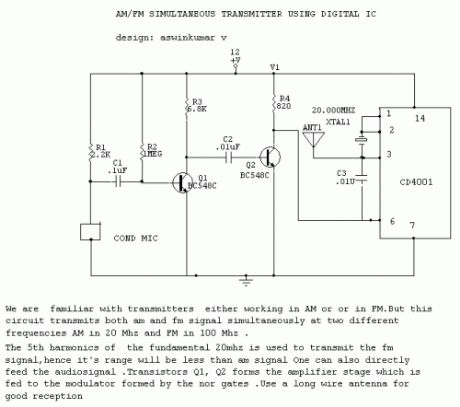
AM FM Simultaneous Transmitter Using Digital IC
Published:2013/7/22 20:04:00 Author:muriel | Keyword: AM , FM , Simultaneous Transmitter, Digital IC
View full Circuit Diagram | Comments | Reading(566)
AM To FM converter
Published:2013/7/22 20:04:00 Author:muriel | Keyword: AM To FM , converter
View full Circuit Diagram | Comments | Reading(699)
Linear FM 50Watt with BLY90
Published:2013/7/22 20:03:00 Author:muriel | Keyword: Linear , FM, 50Watt, BLY90

A amplifier of force RF for the FM, is always essential for the amateur that wants it strengthens some small transmitter, that likely already it has manufactured or has been supplied ready. The present circuit can give 50-60W RF force of expense, with control smaller than 15-20W in the region of frequencies of FM, that is to say in the 88-108MHZ. Transistor that we selected for this manufacture is the BLY90, that has gain 5dB.
As it appears in the analytic drawing (image 1) the amplifier is manufactured with transistor TR1, type BLY90 of Philips. The transistor this is specifically drawn for operation in frequencies up to 175MHZ, with very good results of linearity and record of force. In his technical' characteristics they are included the tendency of operation in the 12V the current of collector in the gain expense in the 5dB (measured in order C) and force of entry in the 16W. Variable capacitors C1, C2, with inductor L1, constitute the circuit of co-ordination, that adapts the exit of our transmitter in amplifier RF. This circuit has been calculated suitably, so that it covers all band the FM with the biggest possible output.Inductor RFC1 polarized the transistor, so as to it works in order C, that is to say with the biggest output. Inductor L2 in the collector of TR1, constitutes the charge of amplifier, while RFC2 prevents the RF signals leak in the line of catering. Capacitor C2 and resistance R1, protect the circuit from auto polarization. The coordinated circuit of expense that is constituted by inductor L2 and variable capacitors C3, C4, adapts the exit of amplifier RF with the next stage, which can be constituted from some amplifier RF of high force (> 300W) or a aerial. This circuit can be supplied with 12V f.e from the battery of one automotive, so that it renders the system emitter portable. Thus, easily it can be moved in points with bigger altitude, in order that from there are achieved radio transmissions, something that was also got used in the past by romantic amateur of radio band. The manufactureThe manufacture of amplifier, is very simple and easy, it is enough to look the images 3 and 2 that portray pcb the amplifier and the placement of materials in this. Puncture the point pcb, that pass the nutshell of TR1. Sticks the capacitors, variable, the resistance, RF tsok and the inductors. Finally you stick TR1, being careful not overheating at the welding and bend the pins his. Clean finally pcb from the residues of iron. Make a very careful control for by any chance errors, omissions, short-circuits, chills you stick also anything other that could you make think that will not work the amplifier.
If all they are it includes, you connect the exit of your transmitter (15-20W) in input the amplifier. The exit of amplifier him you will connect in some charge (dummy load) or in the aerial, through bridge stagnant waves. Supply with tendency 11-15V your amplifier (power supply it should gives current 4-5A). Regulate the 4 variable C1-C4, until you take the biggest force of expense. The amplifier is ready.
Note:TR1 needs a wiper of dimensions 5x10cm for trouble free operation. This wiper in TR1, without insulator, after his central screw has electric isolation from remainder pins.
PartsC1-C4 = 10-80pF C5 = 10nF C6 = 1000pF C7 = 100nF C8 = 2200mF/35V L1 = 1 coils of diameter of 10mms, 1mmL2 = 7 coils of diameter of 10mms, 0,8mmsL3 = 3 coils of diameter of 10mms, 1mmTR1 = BLY90 (View)
View full Circuit Diagram | Comments | Reading(960)
Small Radio Transmitter
Published:2013/7/22 20:02:00 Author:muriel | Keyword: Small Radio, Transmitter
Contains information about building a small radio transmitter, which has a PCB 1.75 x 2.5 (45mm x 68 mm) and has a range of about 30 yards or so. The documentation with the circuit says the freq range is 100-108 MHz, but I have found it to be more like 85-100 MHz.The circuit is (of course) only mono, and accepts an audio input from either a microphone or other source. The input impedance is 1Mohm. The input sensitivity is 5mV and the max input signal is 10mV. The transmitted signal can be picked up on a FM radio. The circuit can be used for short-range transmission, eg. for wireless microphones.The actual circuit comes from a 'Kit', available from Veleman electronics (USA distributor is Tapto Corp., PO Box 1339, CLAREMONT NH-03743-US. UK distributor is High-Q Electronics, 382 Edgware Road, London, W2 1EB). The kit number is K1771. It is a very good transmitter.I bought the kit, and made the circuit, which worked very well. I wanted two transmitters, so I made my own 'copy' PCB and built the circuit, and in fact my home-made version seems to work better than the original!! So there is no need to buy the kit really, as it is quite a simple circuit, and is the best 'home-made' transmitter I have seen.CIRCUIT.GIF is the circuit diagram.PCBPLAN.GIF shows the PCB layout from above (components shown). PCBPLAN.GIF is an accurate layout, scanned from the instruction sheet. I have used * to mark one corner for reference.TRACKS.GIF shows the track layout on the soldering side of the board. This is NOT a very accurate layout. This is because I didn't actually have a plan of the track layout. To get TRACKS.GIF, I put a bit of OHP film onto the bottom of the PCB, and traced the tracks with an OHP pen. I then scanned this in. I have marked the component leg holes (approximately) with white blobs.CONSTRUCTIONStart off by scaling PCBPLAN.GIF and TRACKS.GIF by the same amount so that they measure approximately the correct size (1.75 x 2.5 ) when printed out.Then make your PCB. As mentioned earlier, PCBPLAN.GIF gives the accurate positioning of the holes, whereas TRACKS.GIF gives the positions only approximately. So use PCBPLAN when drilling the holes in your PCB board. Then draw on the tracks, using TRACKS.GIF as a guide. The important thing is to make sure you draw the 'printed coil' correctly on the PCB - those lines are there for a reason!
PartsD1 Varicap diode (eg. BB119)D2 1N4148R1 100KR2 220KR3 22RR4 1K trimmerR5 1KR6 56KR7 1MR8 1K2C1 5pF ceramicC2 6pF ceramicC3 15pF ceramicC4 trimmer capC5 15pF ceramicC6 1nF ceramicC7 100uF electrolyticC8 4.7uF electrolyticC9 100pF ceramicT1 BF244A or BF245A FETT2 2N3819 FETT3 BC307/8/9 or BC557/8/9 PNP
Bear in mind that in addition to the components, there is a jumper wire which needs to be fitted (marked with a dashed line in PCBPLAN.GIF).The power supply to use is 9-14 V DC, one of the little rectangular 9V batteries is fine. Connect this to the + and - points on the PCB. The sound input goes to the points marked MIKE . The antenna should be connected to the point marked ANT . The emitter's output impedance is 50 ohms. You can make your own fancy antenna if you like, but I have found that a foot or so of wire is fine.Good luck with the transmitter. If you have any improvements to the circuit, I would be glad to hear from you. --Dan Evans.
(View)
View full Circuit Diagram | Comments | Reading(445)
4W FM Transmitter
Published:2013/7/22 19:58:00 Author:muriel | Keyword: 4W, FM, Transmitter
TECHNICAL CHARACTERISTICS:Stabilised tendency of catering: Vcc=12~16VFrequency of emission: 88~108MHzConsumption: 100~400mA
Materially:[color=green]The resistors are 1/4W.[/color]R1, R2 10KOhmR3 47OhmC1, C2 1nFC3 4,7uF/16VC4, C7, C8 0~45pF trimmerC5, C6 10pFC9 100nFL1 4 turns, 7mm diameter *L3 3 turns, 7mm diameter *L4 5 turns, 7mm diameter *L2 RFC (resistance 1MOhm with wrapped around her inductor of enough coils from fine isolated wire. Scratch of utmost inductor and you stick in utmost the resistance making thus a parallel L-r circuit.)T1, T2 2N2219ANT Simple dipole l/2.MIC IN Microphone dynamic or other type. (It can also connected to a cassette player unit)[color=green]* The inductors is air from wire of coaxial 75W or other 1mm roughly.[/color]
PCB:Before you print it out with microsoft paints, set the screen resolution to 1280 by 1024 in order to get the correct scale (View)
View full Circuit Diagram | Comments | Reading(493)
20dB VHF Amplifier
Published:2013/7/22 19:57:00 Author:muriel | Keyword: 20dB , VHF Amplifier

Many times we needed to strengthen a small signal in the region of VHF or FM, or it is we lead a body, or a receptor. The preamplifier that to you we propose offers 20dB in all the region of VHF and it still can reach also their 500MHZ. The amplifier is a circuit of high frequency RF with distinguishable materials. The amplifier as circuit strengthens the tendency of signal with concrete aid, depending on the frequency of signal. If the frequency of signal is included in the limits of spectrum of frequencies of amplifier, then it is strengthened, otherwise it is downgraded. Each amplifier of this category, accordingly with his designing, strengthens a concrete region of frequencies and obeys in same characteristics. The one that to you we present today concerns the regions of VHF where they exist and the corresponding television stations for channels 5 until 12. His circuit he is enough simple, so that it is made easily with materials that exist in the trade. It is based on transistors with aid until the 500MHZ. The type of transistor can be BF197 or some other.
In form 1 appears the theoretical circuit of amplifier. As we see it is constituted from two similar circuits (rungs). In this circuits are not included in joint action circuits. With that way is covered a wide spectrum of frequencies, without is differentiated abruptly the aid as for the frequency. With this provision we have smaller gain but big breadth of frequencies. The two rungs are same, with the same prices of materials and each rung offer aid roughly 10dB. The transistors and the remainder materials, because the industrial manufacture, have almost the same characteristics. Associates the particular characteristics of demagogues are altered mainly the aid of rung. Each rung uses a transistor of type npn in provision of common emitter that functions in order A. his rungs works in provision of common emitter with null resistance in emitter. In each rung a network of resistances between the collectors and the bases polarize the transistors and ensures the operation of circuit. The junction between the rungs becomes via ceramic capacitors of small capacity from 0,1nF until 0,22nF (at preference ceramic). In the place of two rungs we can try various transistors of independent company or even different between them. The circuit of course cannot work with all of them. The tendency of catering should emanate from stabilised power supply with tendency 12V. Depending on the tendency of catering and the type of transistor, in each rung of amplifier it needs enter also different resistances. Force of expense, under conditions of high excitation it can exceed the 1 mW
Manufacture The total aid of circuit, according to the elements of transistors, reaches 20dB. Enough aid for a lot of applications. The amplifier is drawn in order to it has big response of frequency up to 0,5Ghz. According to the particular characteristics of manufacture, the better application that we could to you propose for this designing would be the aid of television signal emanating from a small transmitter of television or the preamplifier of a frequency meter. The assembly of amplifier is realised above in printing form 2. In this you will place all the materials according to form 3. The manufacture, in order to it works right it needs one small stabilised power supply 12V. The consumption of circuit is small hardly some mA. The resistance en line with the collector is 10 000. When you finish the construction and the control of manufacture, place the PCB in metal box of suitable dimensions. PartsR1 1KC3 120pFR2 47KC4 150pFR3 1KC5 0,1uFR4 47KC6 120pFC1 150pFC7 150pFC2 0,1uFQ1 Q2 BF197 (View)
View full Circuit Diagram | Comments | Reading(1383)
Medium range transmitter
Published:2013/7/22 19:56:00 Author:muriel | Keyword: Medium range, transmitter

This is a medium range transmitter circuit diagram. This is also improved by changing the values of the resistor. (View)
View full Circuit Diagram | Comments | Reading(359)
| Pages:70/2234 At 206162636465666768697071727374757677787980Under 20 |
Circuit Categories
power supply circuit
Amplifier Circuit
Basic Circuit
LED and Light Circuit
Sensor Circuit
Signal Processing
Electrical Equipment Circuit
Control Circuit
Remote Control Circuit
A/D-D/A Converter Circuit
Audio Circuit
Measuring and Test Circuit
Communication Circuit
Computer-Related Circuit
555 Circuit
Automotive Circuit
Repairing Circuit