Circuit Diagram
Index 1957
TC99ON, TC909OF comb filter integrated circuit
Published:2011/5/4 9:31:00 Author:TaoXi | Keyword: comb filter

The TC99ON and TC909OF are designed as the comb filter integrated circuit which is produced by the TOSHIBA company, and this device can be used in variety of domestic and imported TVs such as the Changhong NC-6, CN-7.etc.
The TC9090N and TC9090F are in the 28-pin dual in-line package, the pin functions and data is as shown in table 1.
Table 1. The TC9090N, TC9090F IC's pin functions and data (View)
View full Circuit Diagram | Comments | Reading(514)
light off reminder circuit composed of 555
Published:2011/5/4 9:28:00 Author:TaoXi | Keyword: light off, remind

The light off reminder circuit composed of 555 is as shown. This circuit is composed of the monostable delay circuit, drive circuit, buzzer, LED.etc. The output signal of the monostable delay circuit which is composed of the 555 and R1、C3 control the other circuits.
After turned on the light, power of the direction light relay adds to the pin-8 of 555 by diode, so the capacitor C3 is charged by R1. Pin-6's electric potential increases, when the pin-6's electric potential increases to 2/3VDD, 555 overturns and pin-3's output low-level voltage makes BG turn on. And this low-level voltage drives the LED to turn on to remind the driver turns off the light. (View)
View full Circuit Diagram | Comments | Reading(1128)
Yadu ultrasonic wave remote control switch circuit
Published:2011/5/4 9:30:00 Author:TaoXi | Keyword: Yadu, remote control, ultrasonic wave

The Yadu ultrasonic wave remote control switch circuit is as shown:
(View)
View full Circuit Diagram | Comments | Reading(415)
TC4052B, TC4052BP double 4 to 1 analog switch circuit
Published:2011/5/4 9:32:00 Author:TaoXi | Keyword: double 4 to 1, analog switch


The TC4052B and TC4052BP is one kind of double 4 to 1 analog switch circuit which is produced by the TOSHIBA company, and they can be used in TV sound system, music center system and other systems as the multi-channel audio signal switcher.
1.TC4052B/BP circuit block diagram and pin functions
The TC4052B and TC4052BP has the same block diagram, as shown in figure 1, they are in the 16-pin double row package, the pin functions and data is as shown in table 1.
Figure 1. TC4052B/BP circuit block diagram and pin functions
Table 1. The pin functions and data of the TC4052B
2. TC4052B/BP typical application circuit
The typical application circuit of the TC4052BP is as shown in figure 2. It can be used in Changhong NC-3 Color TV's Kara OK circuit as the Kara OK mode switching typical application circuit.
Figure 2. TC4052B/BP typical application circuit
3.Circuit process
Add the signal R to pin ①, pin ②, pin (15) of the TC052BP, Signal L add to the pin-11, pin-12 and pin-4 of the TC052BP. Signal R outputs from pin-3 and signal L outputs from pin-13.
Relationship between the TC4052BP signal and Kara OK mode is as shown in table 2.
(View)
View full Circuit Diagram | Comments | Reading(6662)
increase to the active subwoofer amplifier (TDA7294) circuit
Published:2011/5/4 9:45:00 Author:TaoXi | Keyword: increase, active subwoofer amplifier

This circuit updates the audio circuit which uses the IC TDA7294. Pin-10 of the TDA7294 has the mute function, when the external power supplies the high-level voltage, the manifold is in working condition; when the external power supplies the low-level voltage, the manifold turns off, at this time the circuit power consumption is very small, pin-14 of IC1 has no output ( Standby mode). General circuits supply the high-level voltage to the pin-10 to keep it in the conduction mode, by developing this pin's functions, you can make it to meet some special requirements for work. That's why this circuit can makes the active subwoofer amplifier to have the function of standby, the circuit is reliable and responsive. (View)
View full Circuit Diagram | Comments | Reading(12549)
TB31224 communication RF complex integrated circuit
Published:2011/5/4 10:03:00 Author:TaoXi | Keyword: communication, RF, complex


The TB31224 is the communication RF complex integrated circuit that can be used in various models of cordless telephone.
1.Features
The TB31224 is composed of the transmit and receive signal processing circuit, the phase-locked loop signal processing circuit, the audio compression and expansion circuit, the double-conversion processing circuit.etc. This circuit can completes the receive demodulation, PLL control and language processing & compression & extension functions.
2.Pin functions and data
The TB31224 is in the 48-pin package, and the pin functions and data of the host RF complex integrated circuit TB31224 is as shown in table 1. The mobile phone RF integrated circuit TB31224's pin functions and data is as shown in table 2.
Tips: TC31224's pin functions and data is the same as the TB31224's, they are the interchangeable devices.
Table 1 pin functions and data of the host RF complex integrated circuitTB31224
Table 2 The pin functions and data of thecellphoneRF complex integrated circuitTB31224 (View)
View full Circuit Diagram | Comments | Reading(942)
Pincushion Correction Circuit-Discrete Circuit Diagram
Published:2011/5/4 8:17:00 Author:Robert | Keyword: Pincushion Correction, Discrete


It is the parabolic wave signal addedon the r520, and the user can adjust the parabolic wave signal amplitude by adjusting the r520, which canadjust the pincushion correction value as well. It is DC voltage added on the r523, and the user can adjust the line width by adjusting r523.
This second circuit extracted from the Venus d2918 type pincushion correction circuit, whichhasjust V951 and v950 two-stage amplification more than the firstpincushion correction circuit shown below. The reason is that the field sawtooth wave is not taken from field deflection coilssampling resistor, but from tda8838's 46 foot, so thatit'sadded a two-stage amplification due to its small magnitude.
The models which use this pincushion correction circuit have: Korea Samsung mc-15 module, Venus c6418, v6458, Peony 64c1, Lehua ct6388w and so on.
The field sawtooth wave voltage is send to the pincushion correction circuit from the p404's 4 foot, and the r455, c454, r457 make up the integral circuit to integrate the field swatooth wave and produce the up-convexparabolic wave voltage. This voltage then is added on the b polar of the parabolic wave shaping and amplifying tube. Afteramplifying and shaping the c polar output 9V (peak-peak value) down-convex parabolic wave voltage. Then after the level width adjustment, left-rightpincushion distortion adjustment network made up by the vr451, vr452, r464, r463, r462, this voltage wave is added to the polar of the compound tube made up by q453 and q452. After amplifying the q452's c polar outputs 12.5V (peak-peak value) parabolic wave voltage. At last this voltage wave is send to the line scan circuit from fr459 and p403's 3 foot to modulate the line scan current. So this process achieve the goal of pincushion distortioncorrection.
The vr451 is theline width adjustment potentiometer, thevr452 is pincushion distortion correction potentiometer.
(View)
View full Circuit Diagram | Comments | Reading(1482)
Digital displaying remote control electric fan circuit diagram
Published:2011/5/4 3:55:00 Author:Ecco | Keyword: Digital , displaying, remote control, electric fan

Remote control fan circuit is shown as the chart, the remote distance is about 8m, and it does not need dedicated remote control. With an infrared remote control at any infrared receiver by pressing a key, IC2 will receive the infrared pulse signal, and make filter, detect, amplifier and other processing, the signal is coupled to IC3 by C6, Schmid special trigger composed of IC3 and will make shape on pulse signal to obtain the ideal square wave. R1 is pull-up resistor, the appropriate resistance can greatly improve the circuit's noise immunity. The resistance of R1 is in the range of 200kΩ ~ 470kΩ, R1 is too small to reduce the circuit sensitivity; too high to reduce the general assembly performance. After shaping the pulse signal, it is output from 3 feet, and then carried into the CD4017 decade counter to make pulse count. The output end Q0 of CD4017 outputs high level, others outputs low level. The output high level is sent to be decoded by diodes, the driver CD40110 makes the digital display 1.
(View)
View full Circuit Diagram | Comments | Reading(1506)
Brightness Control Relay Circuit
Published:2011/5/4 21:48:00 Author:chopper | Keyword: Brightness Control, Relay

As shown in figure is a brightness control relay circuit.Resistance R1, R2 and photoresistance R3 form a divider circuit.When the light isdark to a certain degree,base voltage of VT1 increases,making the VT1 and VT2 connected,and relay J merged.R1 is used for sensibility control.The light-triggered pedestal of this circuit is influenced greatly by voltage and ambient temperature. (View)
View full Circuit Diagram | Comments | Reading(766)
Parallel Capacitor Circuit
Published:2011/5/4 8:19:00 Author:Robert | Keyword: Parallel, Capacitor


1.Parallel Capacitor
The simplestturn-off snubber circuitis to add the switch with a parallel capasitor Cv, which is shown in picture 1 (a), to limit the rising speed of the switch tubevoltage during its closing time which is shown below. The current before the switch tubeclosed is Io. The more Cv is, the slower therising speed of the switch tube voltageis, and the less power consumption of switch would be. The picture 1(b) and (c) shows the Uv, Iv and P during the closing time in separately. The picture 1 shows the parallel capacitor of the switch tube in the buck converter.
(View)
View full Circuit Diagram | Comments | Reading(585)
photoelectricity control power supply socket circuit diagram
Published:2011/5/4 7:55:00 Author: | Keyword: photoelectricity, power supply socket

This set uses common flashlight beam as remote control instruction,making a conntrolled electric equipment socket, which is can control electric equipment socket power supply on/off in a few meters by touch flashlight switch conveniently.IC can use AN7812、LM7812、W7812 etc type interchangeably.Current amplification factor β of VT1~VT3 is about 200.RL1 and RL 2 can select MG44-03 type plastic resin encapsulation photosensitive resistant, or use other common photosensitive resistant that light resistant≤5kΩ,dark resistant ≥1MΩ instead.T is a 8W~10W power tranformer.
(View)
View full Circuit Diagram | Comments | Reading(1311)
TSV type temperature sensor measurement diagram using constant current
Published:2011/5/4 7:47:00 Author: | Keyword: temperature sensor, constant current

In a TSV type temperature sensor measurement diagram using constant current, when using constant current as load , the load current will not change,voltage drop of lead wire is a constant,so the ouput voltage will change according to10mV/℃.Usually control distant can reach up to thousand meters.
(View)
View full Circuit Diagram | Comments | Reading(416)
Snowflake BCD-251 fridge circuit diagram
Published:2011/5/4 7:43:00 Author: | Keyword: fridge, circuit
View full Circuit Diagram | Comments | Reading(441)
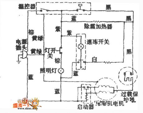
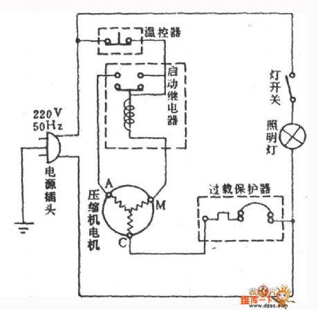
Shasong BC-140 fridge circuit diagram
Published:2011/5/4 7:42:00 Author: | Keyword: fridge, circuit
View full Circuit Diagram | Comments | Reading(491)
High Input Impedance of Broadband Amplifier Circuit
Published:2011/5/4 7:30:00 Author:Joyce | Keyword: High Input, Impedance, of Broadband, Amplifier, FX110

High input impedance of broadband amplifier circuit is shown in the graph below.The first level is a voltage follower, with the typical value of input bias current 1nA ,difference-mode input resistance 1012Ω, input capacitance 1.5 pF and small signal bandwidth 20MHz. The second level has negative feedbacks, and C2 will constitute a feed-forward compensation. The potentiometer is used to adjust the offset voltage of FX110.The accuracy of resistance R1, R2 is 1%. (View)
View full Circuit Diagram | Comments | Reading(503)
TDA8946J two-channel BTL audio power amplifier integrated circuit diagram
Published:2011/5/4 21:34:00 Author:Ecco | Keyword: two-channel, BTL, audio , power amplifier, integrated

TDA8946J is the BTL is audio power amplifier integrated circuit produced by Philips, it is widely used in high-fidelity home theater, television sound audio, multimedia audio and noon and so on. 1. Features of functionTDA8946J integrated circuit contains two BTL circuit with the same function, static noise and the standby control circuit, thermal protection and short protection circuit. When Vcc = 8V, RL = 8Ω, each channel output power is 15W. 2. Pin functions and data TDA8946J IC uses the package with 17 pin in single row, the pin functions and data are listed in Table 1. Table 1 shows TDA8946J integrated circuit pin function and data.
(View)
View full Circuit Diagram | Comments | Reading(1596)
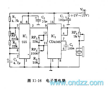
555 Electronic flute circuit
Published:2011/5/4 21:03:00 Author:Ecco | Keyword: 555, Electronic flute

The circuit shown in Figure 11-16 includes the timer and voltage-controlled oscillator. IC1 (555) and R1, RP1, R2, C2 form astable multivibrator, f = 1.44 / (R1 + RP1 +2 R2) C2, the oscillation frequency and duty cycle can be changed by adjusting RP1. IC2 (CD4046) is the CMOS-type phase-locked loop (PLL), the center frequency of voltage-controlled oscillation depends on the external components, sucn as C4, RP2, RP3, R3. The center frequency fmin = 1 / (RP3 + R3) C4, fmax = 1 / (RP2 + RP3 + R3) C4.
Adjusting RP2, RP3 can change the two tones of the electronic flute, adjusting RP1 can change the changing rate of two tones.
(View)
View full Circuit Diagram | Comments | Reading(2143)
TBA800 5W Amplifier Circuit
Published:2011/5/4 8:48:00 Author:Robert | Keyword: 5W, Amplifier

TBA800 5W Amplifier Circuit is shown below.
This circuit's technical data is concluded here:
Output voltage, V: U12 12(11~13)
Static Sink Current, mA:I1+I3 9(<20)
Input DC current, uA: I8 <5
Output power, (Distortion coefficientk=10%), W: Po >4.4
Input AC voltage (Po=5W), mW:U8 80
Input resistance, MΩ:r8 5(>1)
Bandwidth (3dB down),Hz: f3dB 40~20000
Distortion coefficient(Po=0.05~2.5W),%k: 0.5
Voltage gain, dB, with feedback:Vu 42(39~45); without feedback:Vu 80
Input port Noise Voltage,uV:Ut 5
Effciency(Po=4W),%:η 70
(View)
View full Circuit Diagram | Comments | Reading(2469)
Integrated Amplifier Circuit
Published:2011/5/4 9:36:00 Author:Robert | Keyword: Integrated Amplifier

The integrated amplifier circuit is shown below. This circuit is specially suit for the car radio circuits. With internal thermal overload protection, its loading resistance is 2Ω and output power is 10W, and its supply voltage range is from 5V to 18V.
(View)
View full Circuit Diagram | Comments | Reading(401)
Stepper Motor Working Timing Waveform Diagram
Published:2011/5/4 10:02:00 Author:Robert | Keyword: Stepper Motor, Working, Timing Waveform

Stepper Motor Working Timing Waveform Diagram is shown below.
According tothe differences of the power turn-onorder of four-phase stepper motor, the working types could be divided into three types: singld four-beat, double four-beat and eight-beat. Single four-beat type's stepper angle is equal with the double four-beat, but single four-beat type's torque is little. Eight-beatworking type's stepper angle is half of the single and double four-beat type's. So, the eight-beat working type couldnot onlymaintain a high torque but also improve the control accuracy.
The single four-beat, double four-beat and eight-beat working type's power turn-on timing waveform diagrams are shown in the picture 2.a, b, c separately.
(View)
View full Circuit Diagram | Comments | Reading(2158)
| Pages:1957/2234 At 2019411942194319441945194619471948194919501951195219531954195519561957195819591960Under 20 |
Circuit Categories
power supply circuit
Amplifier Circuit
Basic Circuit
LED and Light Circuit
Sensor Circuit
Signal Processing
Electrical Equipment Circuit
Control Circuit
Remote Control Circuit
A/D-D/A Converter Circuit
Audio Circuit
Measuring and Test Circuit
Communication Circuit
Computer-Related Circuit
555 Circuit
Automotive Circuit
Repairing Circuit

