
Circuit Diagram
Index 1954
Guangzhou FIT reversing light circuit diagram
Published:2011/5/5 2:51:00 Author:muriel | Keyword: Guangzhou FIT, reversing light
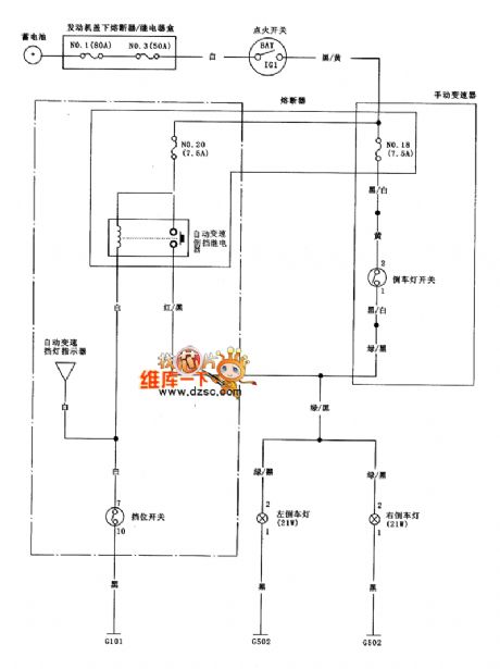
Guangzhou FIT reversing light circuit diagram is as shown
(View)
View full Circuit Diagram | Comments | Reading(432)
Guangzhou FIT embarkation lamp circuit diagram
Published:2011/5/5 2:52:00 Author:muriel | Keyword: Guangzhou FIT , embarkation lamp
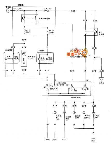
Guangzhou FIT embarkation lamp circuit diagram is as shown
(View)
View full Circuit Diagram | Comments | Reading(527)
Mitsubishi Pajero (PAJERO) light off-road vehicle wiping, washing circuit principle circuit diagram
Published:2011/5/5 2:53:00 Author:Rebekka | Keyword: Mitsubishi Pajero, Light off-road vehicles

50 a front window wiper motor; 51 a front window wiper switch; 52 a front window intermittent wiper relay; 53 washing the front window of a motor; 53 a II the front window washer switch; 54 a rear window wiper motor; 55 a rear window wiper and washer switch; 56 a rear window wash motor. (View)
View full Circuit Diagram | Comments | Reading(1179)
Driver alcohol detection alarm controller circuit
Published:2011/5/5 2:31:00 Author:Christina | Keyword: Driver, alcohol detection, alarm controller

The driver alcohol detection alarm controller circuit is as shown in the figure. The QM-NJ9 is alcohol gas sensor, if it detects the alcohol odor, the resistance of QM-NJ9 between A and B will shrink, and the wiper potential of potentiometer RPl will rise up. When the voltage level is 1.6V, the ICl high-power switching device TWH8778 is connected to make the IC2 voice IC TM801 to work, the output is amplified by the IC3 integrated amplifier LM386, and then the amplified output drives the speaker BLl to send out alarm. Meanwhile, the relay J1 gets the power to start working, the contact point disconnects and cuts off the car ignition circuit to stop the engine, to achieve the purpose of control the drivers drink and drive.
(View)
View full Circuit Diagram | Comments | Reading(5377)
KA2213 single chip sound recorder or reproducer integrated circuit diagram
Published:2011/5/5 2:50:00 Author:Nicole | Keyword: single chip, sound recorder or reproducer


KA2213 is a single chip record and play back integrated circuit which is produced by South Korea's Samung, it is used in recorder and unit audio.
1, KA2213 internal circuit block diagram and pin function
KA2213 internal block contains a record and play back preamplifier, a power amplifier circuit, a automatically gain control circuit(ALC)and ripple filter circuit. The internal block internal circuit block diagram is shown in the figure 1-1. Reading IC adopts 14-foot dual in-line package, it has cooling ribs. The integrated circuit pin function and data is shown in the chart 1-1.
Figure 1-1, the internal block internal circuit block diagram is shown.
2, KA2213 typical application circuit
KA2213 internal block typical application circuit is shown in the figure 1-2. The figure has no flux imbalance circuit. SW1-SW6 is record and play back switch, the graphic position is in sound-reproducing state.
Figure 2-2, KA2213 internal block typical application circuit (View)
View full Circuit Diagram | Comments | Reading(3082)
Based on a pulse regulating neon type switching regulated power supply circuit diagram
Published:2011/4/22 18:53:00 Author:Nicole | Keyword: switching power supply

This is a pulse Ni switching power supply circuit diagram, it is Kaige 4D17U produced by radio four factory in Shanghai. The power supply of 35cm black and white TV.
The main technical indicators are as follows: Output voltage: 12V; Output Current: 1A; power consumption <20W; efficiency> 64%; resistance <0.075Ω; ripple <15mV; mains voltage: 160 ~ 240V.
As shown, 6VDl, 6VD2 form full-wave rectifier circuit; 6C3is filter capacitor; 6C1, 6C2 are used to weaken the inrush current; 6VT7, 6VT2, 6VT3 and 6R4, 6C9 constitute the self-excited multivibrator, 6VT7 also is the switching tube.
When the 12V output voltage decreases for some reason, the base of error amplification 6VT5 obtain the voltage from the sampling circuit 6R6, 6R9, 6R8 also drop, the collector voltage of 6VT5 rises, potential base 6VT3 increases, the output pulse of switch controls tube 6VT7 widen, then the reducing voltage rises again. On the contrary, to adjust on the opposite by the above process when the output voltage goes down, to make the output voltage stable.
(View)
View full Circuit Diagram | Comments | Reading(1920)
secret code lock circuit
Published:2011/5/5 2:55:00 Author:Christina | Keyword: secret code, lock

Figure: secret code lock circuit (View)
View full Circuit Diagram | Comments | Reading(930)
Long-distance call lock circuit
Published:2011/5/5 2:51:00 Author:Christina | Keyword: Long-distance, lock

The long-distance call lock circuit is as shown, it has the following features: if you want to make a long distance call (the first telephone number is zero), you need to enter the 4-digit password and hang up for 1 ~ 2s then you can make the long distance call; this circuit does not limits the non-long-distance calls (the first telephone number is not zero); you can set any passwords and limit to call the restricted number.
(View)
View full Circuit Diagram | Comments | Reading(551)
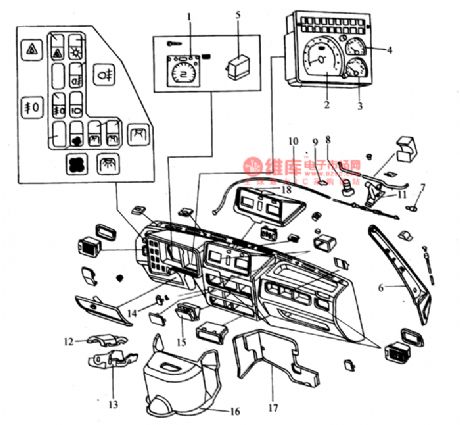
Nanjing IVECO car instrument panel circuit diagram
Published:2011/5/5 2:52:00 Author:Nicole | Keyword: Nanjing IVECO, instrument panel
View full Circuit Diagram | Comments | Reading(1083)
Strong stability boost output circuit diagram
Published:2011/4/7 3:44:00 Author:Nicole | Keyword: boost, output

The figure is a boost output type practical circuit. VT3 is the switching regulator; regulator VD2 can change the potential; VT4 is inverting isolation amplifier; Ui is divided by the VT4 and its 33kΩ load resistor. The two voltage supply for pulse generator circuit. Pulse generator circuit consists of the transformer T and VTl, VT2. This is a non-symmetric transformer feedback self-excited multivibrator. The supply of VTl is from the voltage of 33kΩ load resistor, and the current of resistance depends on the current of VT4. VT1, VT2 have different supply voltage, the oscillation amplitude of half and half weeks is changed in direct proportion, the width is inversely proportional to the change, to control the on and off time of VT3. When the output voltage increases, the differential pair VT6 current of error amplifier increases, VT5 current decreases, the collector potential rise, VT4 current increases, 33kΩ resistor voltage drop increases, VTl pipe supply pressure is increased, conduction time is shortened, the conduction time of switch VT3 is shortened, too.
The circuit input voltage is 12 ~ 28V, the output can be stable for 30V, maximum output power is 60W, efficiency is 89.4% ~ 94.7%, instability is ± 0.33%, the ripple coefficient of output voltage is 0.02%, operating frequency is 10kHz.
(View)
View full Circuit Diagram | Comments | Reading(791)
UV sensor basic circuit
Published:2011/5/5 2:51:00 Author: | Keyword: UV sensor, basic

The basic circuit of UV sensor and it's output waveform is as shown in the picture, in which R1and C1 form the charge and discharge loop circuit. It's time constant is called damping time constant.The decay time of electrode residual ion is generally 5-10ms. When the incident UV flux is below a certain value, there can be obtained a number of pulses from the output proportional to those from the incident flux, but if the flux is larger than this value, due to C1's discharge, the tube current is saturated. Therefore, the UV sensor is suitable to be used as photoelectric switch, while not suitable for precision UV measurement. (View)
View full Circuit Diagram | Comments | Reading(951)
Three-channel audio power amplifier integrated circuit diagram
Published:2011/5/5 2:46:00 Author:Ecco | Keyword: Three-channel , audio, power amplifier , integrated circuit

TDA7494 is the three-channel audio power amplifier integrated circuit produced by Philips, it is widely used in the high-fidelity home theater, television, audio and other systems. 1. Features of functionTDA7494 integrated circuit contains three-way audio power amplifier circuits with the same functions, two independent mute control circuits, it can execute independent mute control on the main channel and sub channel; it also has overheat, short circuit protection functions. 2. Pin functions and data TDA7494 integrated circuit uses the package with 15-pin in single row, the pin functions and data are listed in Table 1. Table 1 shows TDA7494 integrated circuit pin functions and data.
(View)
View full Circuit Diagram | Comments | Reading(948)
The ring flasher principle circuit diagram
Published:2011/5/5 2:41:00 Author:Ecco | Keyword: ring flasher , principle

The circuit shown as the chart is the ring scintillator, it is mainly composed of the NE555, CD4017 and external circuit. NE555 constitutes a multivibrator, its square wave output from pin 3 will control CD4017 decoding output shift to turn on LEDs one by one, so that the LEDs flash in ring. The line flicker frequency shown as the chart is about 1.5Hz, operating current is less than 50mA. Component selection: IC1 selects 555 time base circuit, IC2 selects CD4017 integrated circuit. R1 selects (1 / 2) W metal film resistor, the other resistors choose (1 / 4) W resistors, LED0 ~ LED9 can select Φ5mm super bright red LED. Other components are shown as the chart. (View)
View full Circuit Diagram | Comments | Reading(448)
KA2402-motor speed-stable integrated circuit diagram
Published:2011/5/5 1:44:00 Author:Nicole | Keyword: motor speed-stable


KA2402 is a DC motor speed-stable integrated circuit which is produced by South Korea's Samung, it is widely used in all kinds of super miniature, miniature audio, it is as motor drive circuit.
1, KA2402 internal circuit and pin function
KA2402 integrated block internal circuit and typical application circuit is shown in the figure 1-1. This IC has two kinds of package type, KA2402 is 8-foot dual in-line structure, KA2402 is 8-foot dual line flat type structure. The pin function and data of this integrated circuit is shown in the chart 1-1. The former voltage range is Vcc=1.8-8V, the later is 1.8-5V.
Figure 1-1 KA2402 integrated block internal circuit and typical application circuit is shown.
2, KA2402 typical application circuit
KA2402 integrated block typical application circuit is shown in the figure 1-1. (View)
View full Circuit Diagram | Comments | Reading(1570)
CPU—WT6861/WT62Pl single chip microcomputer integrated circuit diagram
Published:2011/5/5 2:04:00 Author:Nicole | Keyword: single chip, microcomputer


CPU—WT6861/WT62Pl is a single chip microcomputer integrated circuit, as master control chip, it is used in computer multiple frequency color display, such as Tsinghua Tongfang 5E series displays.
1, Function and feature
CPU—WT6861/WT62Pl integrated circuit contains I(2)C total line control circuit, row and field pulse singal process circuit, automatical degaussing control circuit, energy-saving function control circuit, key scanning switch compiling code circuit, memory interface circuit, CPU circuit, S corrective capacity switching control circuit, grating inclination control circuit.
2, Pin function and data
CPU—WT6861/WT62Pl integrated circuit adopts 40-foot DIP, the integrated circuit pin function and data is shown in chart1.
Chart1, CPU—WT6861/WT62Pl integrated circuit pin function and data is shown.
(View)
View full Circuit Diagram | Comments | Reading(656)
The typical application circuit diagram of LA1185 IC
Published:2011/5/5 1:28:00 Author:Ecco | Keyword: typical application circuit, IC

The typical application circuit diagram of LA1185 IC is shown as the chart.
Tip: FM radio signal passes band-pass filter composed of C1, L1, C2, and the signal without FM band is filtered and then coupled by C3, then it is added LA1185 ① feet, it is amplified and added to the mixer oscillator circuit, and it will be made vibration signal mix with the local signal sent by the local oscillator circuit, the resulting difference frequency signal is output from ⑥ feet, and the filter composed of B1 will select 10.7MHz IF signal and send it to later level circuit to do further treatment.
(View)
View full Circuit Diagram | Comments | Reading(4005)
The different lantern signal generation circuit
Published:2011/5/5 2:33:00 Author:Ecco | Keyword: different , lantern , signal generation circuit
View full Circuit Diagram | Comments | Reading(429)
Ring-type switching power supply constant current drive circuit diagram
Published:2011/3/30 3:29:00 Author:Nicole | Keyword: switching power supply, constant current drive

It is essentially a simple series regulator. The load is a fixed resistor RB. Even if the input voltage Ui changes, the current flowing through RB is constant. This will not only significantly reduce the loss of the resistance, but also to prevent intermittent oscillation. AC is in range of 100 ~ 200V, the power can work continuously.
In the ring-type switching power supply, the loss of the drive circuit of supply switching transistor base current is considerable. In addition to ensuring the switching transistor can fully turn with the minimum input voltage, the voltage UB on the transformer winding is in direct proportion to the input voltage Ui. when Ui rises, the drive current Id increases too, and the incremental losses of the base resistance Rb, can increase with the square of increasing part of Id.
When the drive current ID is increasing, the current of the branch of regulator diode must be increased, it may cause oscillation, that is, the switching works in a period of time, but will stop working in the adjacent time. Over and over again, the frequency of oscillation is about several hundred to several thousand Hertz.
To solve these problems, that is, when the input voltage changes, it can adopt constant current drive to remain drive current unchanged, as shown below.
(View)
View full Circuit Diagram | Comments | Reading(885)
STV8223 Intermediate frequency amplifier integrated circuit diagram
Published:2011/5/5 1:33:00 Author:Ecco | Keyword: Intermediate frequency, amplifier, integrated circuit

STV8223 is the intermediate frequency signal amplifier integrated circuit produced by SGS-THOMSON company in French, it is widely used in various domestic and imported large screen color television sets, such as Skyworth, TCL, Rover and other high-color television. 1. Features of functionSTV8223 IC mainly contains the PLL circuit, AV / TV control circuit, 38MHz frequency discriminator circuit, intermadite and high level radioactive AGC circuit, the audio signal amplification circuit, frequency circuit, electronic volume control circuit and other subsidiary function circuit. 2. Pin functions and data STV8223 IC uses 24-pin dual in-style package, the pin functions and data are listed in Table. STV8223 IC pin functions and data
(View)
View full Circuit Diagram | Comments | Reading(607)
STV2180 Color baseband delay line integrated circuit diagram
Published:2011/5/5 1:44:00 Author:Ecco | Keyword: Color baseband , delay line , integrated circuit

STV2180 is the color baseband delay line integrated circuit produced by SGS-THOMSON company in French, it is widely used in various domestic and imported color television sets, such as TCL, High Road, Hua, Skyworth, Hisense and other products. 1. Features of function STV2180 integrated circuit is mainly composed of (R-Y) and (B-Y) signal processing circuit, sand castle pulse signal processing circuit, the delay processing circuit, the buffer signal processing circuit, and other ancillary functions circuit. 2. Pin functions and data STV2180 IC uses 14-pin dual in-line plastic package, the pin functions and data are listed in Table. STV2180 IC pin functions and data
(View)
View full Circuit Diagram | Comments | Reading(500)
| Pages:1954/2234 At 2019411942194319441945194619471948194919501951195219531954195519561957195819591960Under 20 |
Circuit Categories
power supply circuit
Amplifier Circuit
Basic Circuit
LED and Light Circuit
Sensor Circuit
Signal Processing
Electrical Equipment Circuit
Control Circuit
Remote Control Circuit
A/D-D/A Converter Circuit
Audio Circuit
Measuring and Test Circuit
Communication Circuit
Computer-Related Circuit
555 Circuit
Automotive Circuit
Repairing Circuit